

Technical library
Change the rules for semiconductor device designers with DALP® Technology
DALP® Technology (Direct Atomic Layer Processing) is transforming the semiconductor industry by dramatically accelerating the transition from ideas to prototypes.

Browse by category
Technical Library
White papers, application notes, peer-reviewed publications and research articles from ATLANT 3D and our research partners. Choose a category to filter.
Lithography-free patterning of SrTiO₃-based two-dimensional electron gases using direct atomic layer processing
Patterned SrTiO₃-based 2D electron gases written directly, without post-growth microfabrication steps.
Request access → White paper
NANOFABRICATOR® Process and Sample Reproducibility Data
Process stability and run-to-run reproducibility data for NANOFABRICATOR® platforms in MEMS, photonics and microelectronics.
Request access → Publication
Self-aligned patterning by area-selective etching of polymers and area-selective atomic layer deposition: Decreasing polymer flow and activating noncatalytic surface
Combining area-selective polymer etching with area-selective ALD for self-aligned patterning in future device architectures.
Request access → Publication
Optical color structuring via DALP-fabricated thin-film interference cavities in ZnO/SiO₂ on Si
Structural colors from locally deposited ZnO/SiO₂ interference cavities, tuned by ZnO thickness.
Download PDF ↓ Research article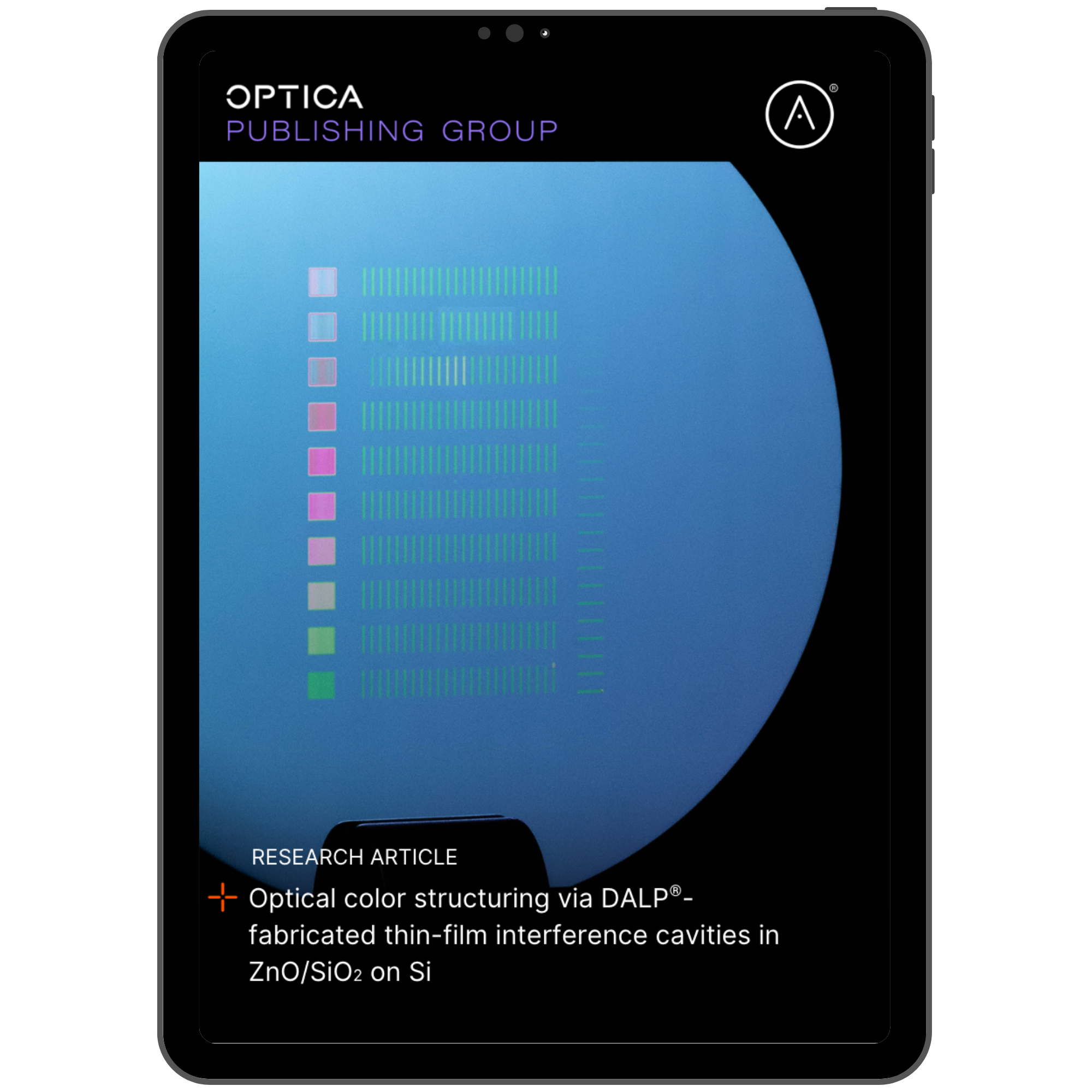
AZO (Al-doped ZnO) Thin Films Fabricated by DALP® Technology: A Combinatorial Approach
A combinatorial study of Al-doped ZnO transparent conductive films for electronic, optical and energy devices.
Download PDF ↓ Publication
Local edge passivation of laser-scribed cells for compensating cut losses
Localized TiO₂ edge passivation with DALP® Technology recovers carrier lifetime and implied open-circuit voltage in laser-scribed TOPCon cells.
Download PDF ↓ Publication
Growth dynamics in patterned TiO₂ deposited by direct atomic layer processing (DALP) in ambient conditions
How patterned TiO₂ grows when deposited by DALP® Technology in ambient conditions, compared with vacuum-based area-selective ALD.
Read in journal ↗ Application note
Coating Innovations for Micro Devices
Maskless, localized thin-film coatings that extend the lifetime of micro devices while keeping material use and cost low.
Read more → Application note
Optical Filters
Cost-effective, pixelated optical filters for hyperspectral and multispectral imaging, written directly with DALP® Technology.
Read more → Application note
Electrochemical Glucose Sensor
Faster prototyping of electrochemical glucose sensors by depositing functional layers only where the sensor needs them.
Read more → Publication
Direct-Patterning SnO₂ Deposition by Atomic-Layer Additive Manufacturing
Maskless, direct patterning of SnO₂ lines with controlled thickness using atomic-layer additive manufacturing.
Download PDF ↓ White paper
Chip Surgery – Revolutionizing Chip Repair
Repair deposition defects on finished chips in minutes: DALP® Technology adds material exactly where it is missing, without restarting the fabrication process.
Read more → White paper
Platinum Deposition Without Reactant
A reactant-free route to localized platinum films with DALP® Technology, cutting precursor use and process time for catalytic and electronic applications.
Request access → White paper
Change the rules for semiconductor device designers with DALP® Technology
How DALP® Technology shortens the path from idea to prototype for semiconductor device designers.
Read more → PublicationDirect-Patterning ZnO Deposition by Atomic-Layer Additive Manufacturing Using a Safe and Economical Precursor
Direct patterning of ZnO with a safer, lower-cost precursor.
Request access → Publication
Additive manufacturing in atomic layer processing mode
An introduction to atomic-layer additive manufacturing (ALAM) and its ångström-scale vertical resolution.
Request access →
Let’s talk
- Co-develop new materials, processes and devices with our R&D and Applications teams
- Build joint research projects and co-authored publications with DALP® Technology
- Find the right way to work together: a NANOFABRICATOR® platform, an A-HUB project or a research partnership
Talk to us:
Sales Team
sales@atlant3d.comLet’s collaborate on your next material or device
Planning a joint research project, a new application or a publication? Tell us about your challenge and our team will come back to you with the right next step.
Start a projectShare your application with our team Download the Platforms & Applications brochurePlatforms, capabilities and application examples Contact pageAll ways to reach ATLANT 3D
Building the materials of tomorrow.
Atom by Atom®.
Contact us
Have a material, process, or application you want to explore?
Connect with our team to discuss how ATLANT 3D’s technology and platforms could support your materials development needs.
- sales@atlant3d.com
- Mårkærvej 2B, 2630 Taastrup, Copenhagen, Denmark