01
Technology & innovation partnerships
Explore new materials, co-develop processes and accelerate innovation with DALP® Technology.





Applications & industries
One programmable DALP® Technology, applications across industries. From AI-driven materials discovery to semiconductors, sensors, energy, photonics and space, NANOFABRICATOR® platforms place the right material exactly where your device needs it.
Powered by DALP® Technology
The applications on this page are our focus areas, not the limit. DALP® Technology performs atomic layer deposition (ALD) locally and without masks, opening atomic layer deposition applications that blanket films cannot reach. Every one runs on the same direct-write, atomic-scale process, and because recipes are defined in software, DALP® Technology adapts to new materials, devices and industries, moving from exploration to production across the NANOFABRICATOR® family.
Localized atomic layer deposition and etching, layer by layer, including programmable thickness gradients.
450+ compatible materials, switched within a single workflow to build complex stacks.
No masks, resist or lithography. Material is processed only where the design places it.
From design to fabrication in hours, with consistent workflows from lab to fab.
Applications & use cases
From materials discovery to advanced manufacturing, DALP® Technology enables next-generation innovation across semiconductors, MEMS, energy, photonics, aerospace and beyond. Explore each area, its key use cases and results achieved on NANOFABRICATOR® platforms.
Application use cases
Combinatorial libraries written on a single substrate, so composition screening and AI-guided iteration run in days instead of months.
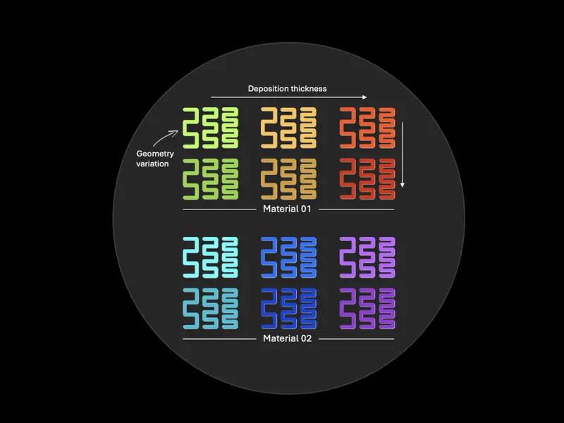 →01Rapid combinatorial material screeningMulti-material atomic-scale fabrication for accelerated materials discoveryClick to learn more →
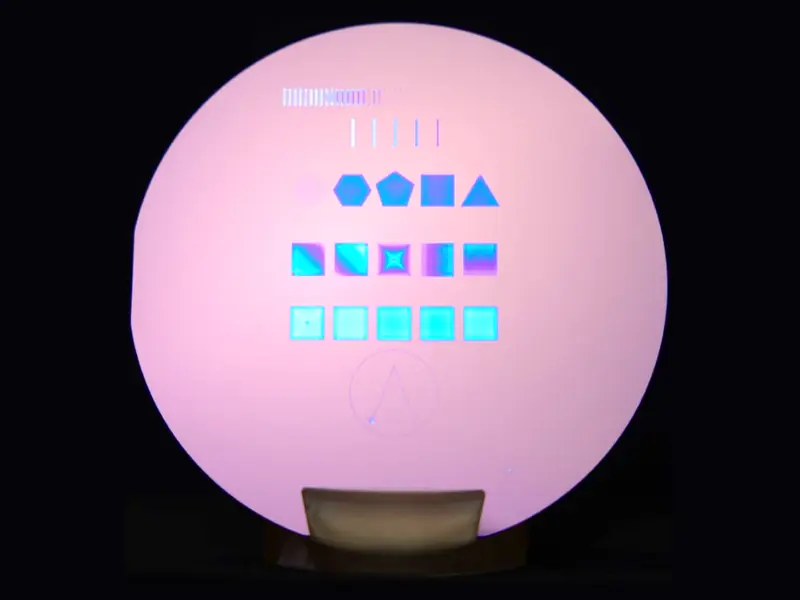 →02Programmable surface structuresPrecise surface patterning for advanced functional surfacesClick to learn more →
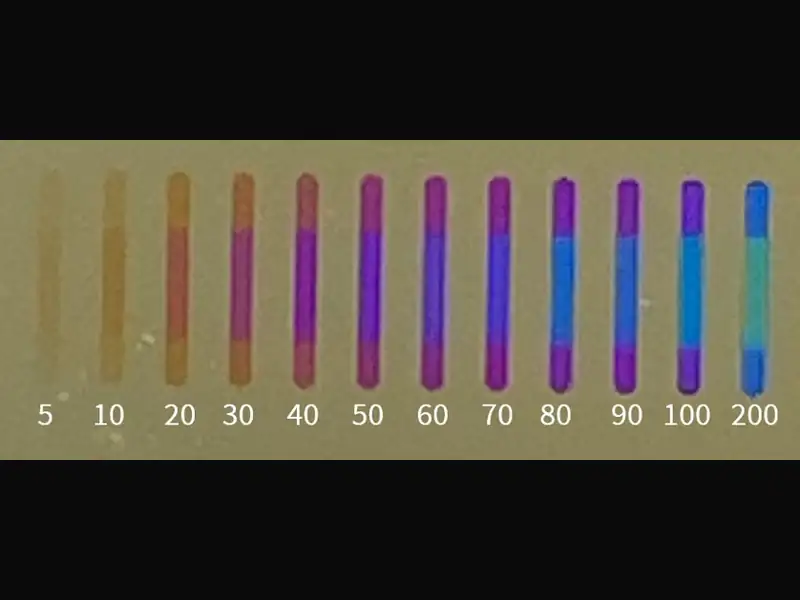 →03AI-driven materials developmentSoftware-defined recipes that turn AI-designed materials into real samplesClick to learn more →
Advanced Materials & Discovery: use cases
Multi-material atomic-scale fabrication for accelerated materials discovery
The challenge: Optimising deposition conditions for a new material traditionally means one recipe, one wafer, one measurement at a time. Each iteration costs days, making materials discovery slow and resource-intensive.
How DALP® Technology solves it:
Results:
6 Hours vs. 1–2 weeks for 50 data points
Precise surface patterning for advanced functional surfaces
The challenge: Functional surfaces such as metasurfaces or hybrid bonding interfaces need tailored nanoscale topographies. Producing many pattern variants with conventional thin-film processing requires separate masks and process runs for each design.
How DALP® Technology solves it:
Results:
1 substrate, many pattern designs
Software-defined recipes that turn AI-designed materials into real samples
The challenge: Materials and device development is limited by how fast high-quality experimental data can be generated. Sequential trial-and-error cannot feed AI models with the volume and consistency of data they need.
How DALP® Technology solves it:
Results:
50+ variants per wafer
Application use cases
Ultra-thin functional films only where they are needed, on edges, bond areas and selected die regions, with no added lithography.
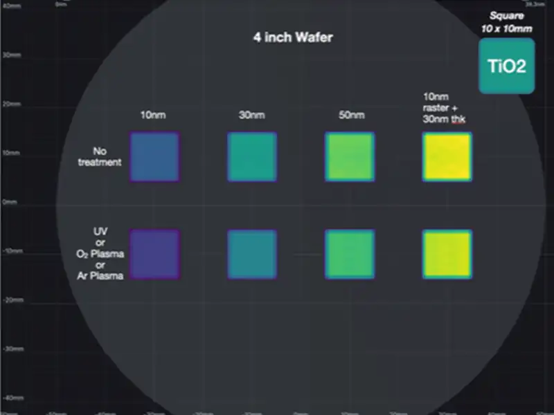 →01Camera module bonding & surface optimizationAtomic-scale surface engineering for high-yield electronics manufacturingClick to learn more →
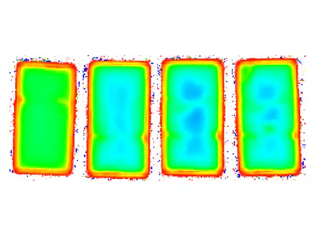 →02Localized edge passivationLocalized atomic-layer edge passivation for advanced solar cellsClick to learn more →
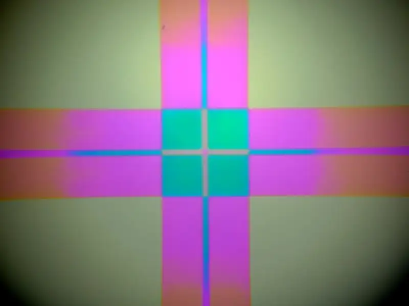 →03Chiplet & heterogeneous integrationLocalized layers for multi-die and hybrid integrationClick to learn more →
Semiconductors & Advanced Packaging: use cases
Atomic-scale surface engineering for high-yield electronics manufacturing
The challenge: Camera bonding attaches the cover glass to the lens barrel in high-volume smartphone module assembly. Conventional processes apply excess adhesive, driving misalignment, contamination, rework and material waste at very large scale.
How DALP® Technology solves it:
Results:
90% less adhesive waste
Localized atomic-layer edge passivation for advanced solar cells
The challenge: Edge passivation improves the performance of semiconductor devices and solar cells, but coating only the edges is difficult. Conventional flows coat the entire substrate and then remove the layer from front and back, requiring multiple deposition, lithography and etch steps.
How DALP® Technology solves it:
Results:
1.5 Hours single-step edge passivation
Localized layers for multi-die and hybrid integration
The challenge: Chiplets, 3D ICs and large-panel packaging need functional layers in very specific places: on die edges, inside vias, or around critical features. Blanket deposition plus masking adds steps, cost and risk to already complex assembly flows.
How DALP® Technology solves it:
Results:
0 masks needed
Application use cases
Dielectrics, metals and oxides written directly onto finished, fragile devices, and multi-material sensor arrays in one process.
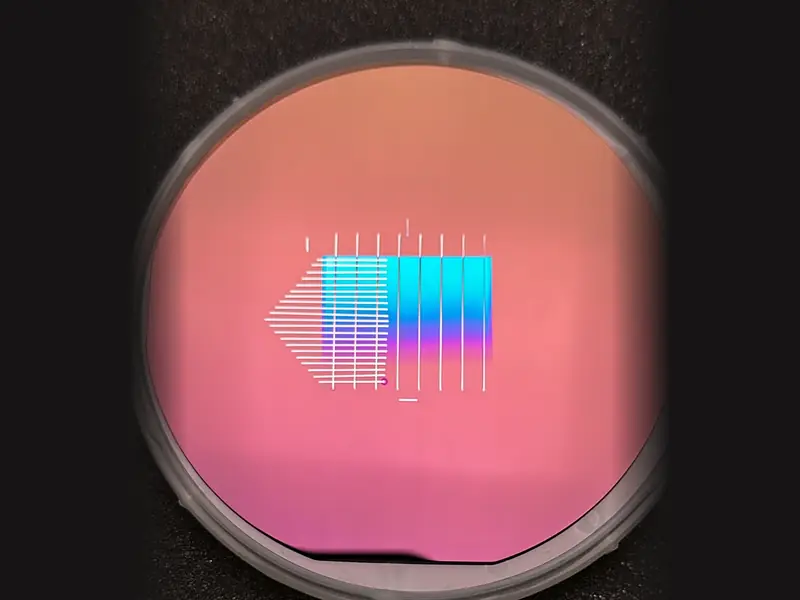 →01Integrating 2.5D capabilities in device designProgrammable gradient structures for advanced electronics and sensingClick to learn more →
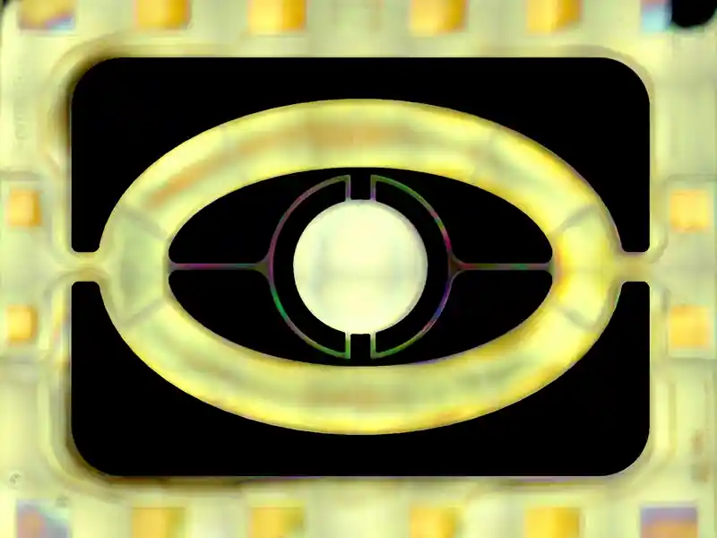 →02Advanced packaging for MEMS & opticsDirect dielectric patterning for suspended MEMS structuresClick to learn more →
 →03Multi-gas & electrochemical sensorsSeveral sensing materials written on one chipClick to learn more →
MEMS & Sensors: use cases
Programmable gradient structures for advanced electronics and sensing
The challenge: Gradient and step structures hold unique potential for electronics, optics and sensing, but they are very difficult to produce with traditional thin-film processing.
How DALP® Technology solves it:
Results:
60 MIM capacitors on one chip
Direct dielectric patterning for suspended MEMS structures
The challenge: Protective coatings on suspended MEMS structures such as micromirrors must avoid critical device areas. Lithography is not feasible because resist spinning would damage the released, suspended structures.
How DALP® Technology solves it:
Results:
0 resist or lithography steps
Several sensing materials written on one chip
The challenge: Conventional gas sensors need one device per gas, limiting scalability and increasing system complexity. Developing multi-sensor arrays is slow and constrained by rigid materials and fabrication processes.
How DALP® Technology solves it:
Results:
1 chip, multiple gases
Application use cases
Screen catalyst and interface variants side by side, and use precious metals only where they add performance.
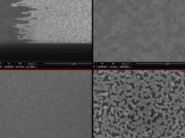 →01Tailoring functional properties across surfacesProgrammable thickness gradients for catalyst and electrochemical materials discoveryClick to learn more →
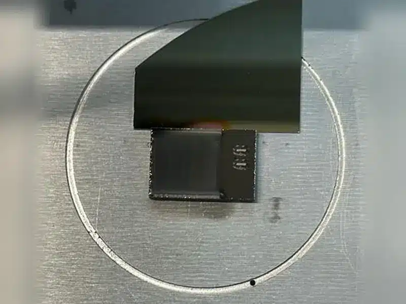 →02Water splitting & H₂ generationLocalized Pt deposition for efficient electrochemical catalyst developmentClick to learn more →
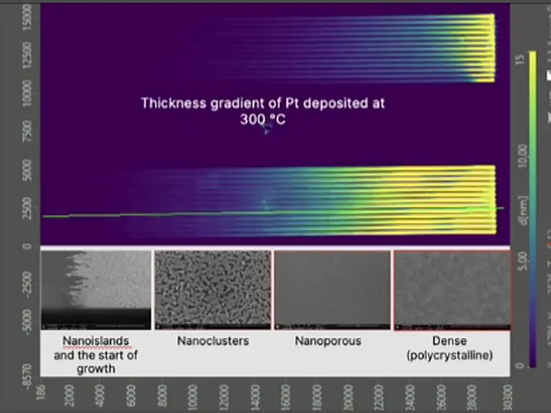 →03Catalyst discoveryPt thickness gradients that map catalyst growth on a single sampleClick to learn more →
Energy & Electrochemical Systems: use cases
Programmable thickness gradients for catalyst and electrochemical materials discovery
The challenge: Catalyst performance depends strongly on film thickness and morphology. Studying this relationship conventionally requires a separate sample for every thickness.
How DALP® Technology solves it:
Results:
60+ thickness steps in one gradient
Localized Pt deposition for efficient electrochemical catalyst development
The challenge: Efficient, durable catalysts are crucial for water splitting, but uniform, well-adhered platinum coatings on complex or microstructured substrates are hard to achieve. Conventional techniques waste expensive Pt and give uneven thickness and poor adhesion.
How DALP® Technology solves it:
Results:
20 nm catalytic Pt layer
Pt thickness gradients that map catalyst growth on a single sample
The challenge: Catalyst activity depends on how a metal film grows, from isolated nanoislands to dense layers. Mapping that evolution conventionally needs a separate deposition and sample for every thickness.
How DALP® Technology solves it:
Results:
1 sample, full growth window
Application use cases
Optical layers, gradients and waveguides written directly from design, so filters and photonic devices are prototyped without masks.
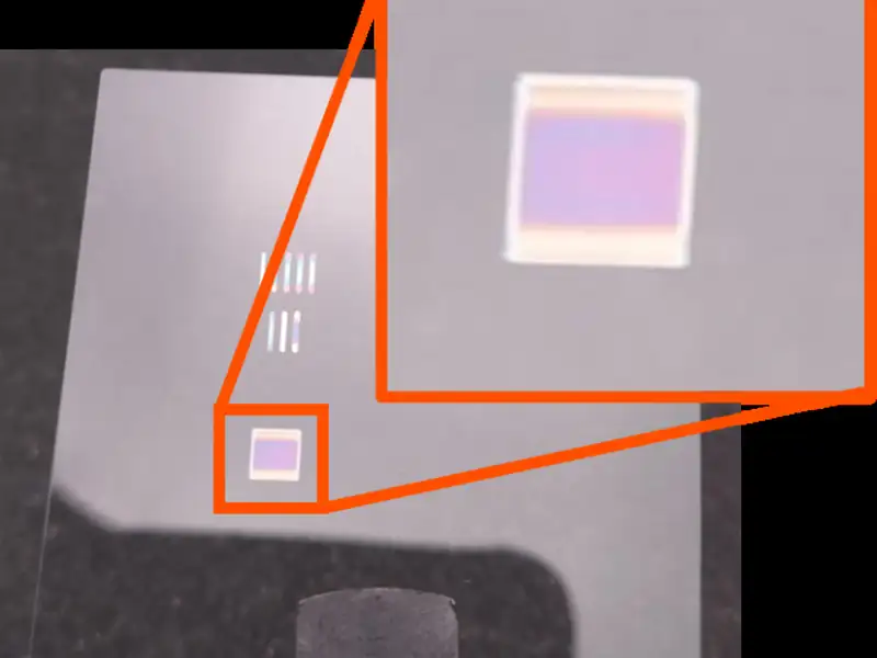 →01Programmable optical filters for multispectral sensingGradient optical structures with tunable spectral responseClick to learn more →
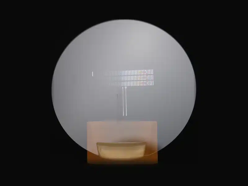 →02Direct write of photonic devices & waveguidesDirect-write fabrication of integrated photonic waveguidesClick to learn more →
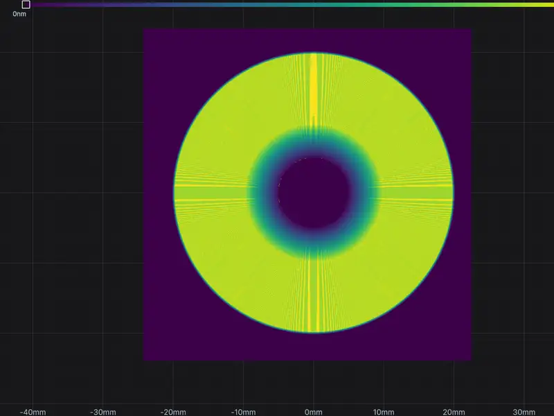 →03Metasurfaces & flat opticsSelective deposition with precise pattern controlClick to learn more →
Photonics & Optoelectronics: use cases
Gradient optical structures with tunable spectral response
The challenge: Optical filters for multispectral and hyperspectral imaging are expensive to manufacture. A filter for a simple CMOS sensor can approach $10k, a major barrier for markets such as waste sorting, agriculture and authentication.
How DALP® Technology solves it:
Results:
≈1 transmission at peak
Direct-write fabrication of integrated photonic waveguides
The challenge: Integrated photonic waveguides are time-intensive to fabricate, require expensive masks and lithography, and make thickness or composition variations difficult to implement.
How DALP® Technology solves it:
Results:
6× faster prototyping
Selective deposition with precise pattern control
The challenge: Novel optical elements require rigid, multi-step fabrication, so typical optical filters can only provide simple gradient structures. Complex radial or freeform profiles are out of reach.
How DALP® Technology solves it:
Results:
Å level height control
Application use cases
On-demand fabrication and repair: on Earth with NANOFABRICATOR® PRO, in orbit with NANOFABRICATOR® ZERO-G.
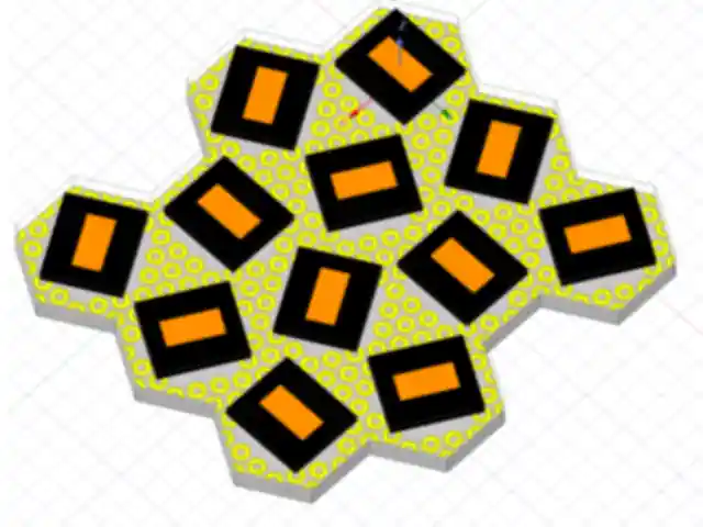 →01RF shielding & antenna module integrationLocalized fabrication of custom metal resonators for RF shieldingClick to learn more →
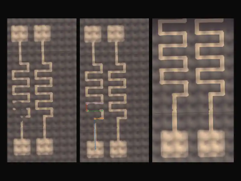 →02Chip surgery & defect correctionReal-time correction of microfabrication defectsClick to learn more →
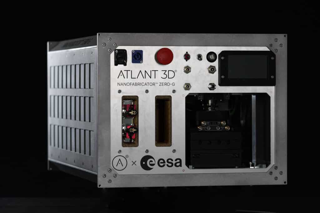 →03In-space fabrication & repairOn-demand parts and chip-level repair in orbit with NANOFABRICATOR® ZERO-GClick to learn more →
Aerospace, Defense & Secure Systems: use cases
Localized fabrication of custom metal resonators for RF shielding
The challenge: Aerospace and defence systems need compact RF shielding and resonator structures close to sensitive electronics. Conventional fabrication adds integration steps and limits where these structures can be placed.
How DALP® Technology solves it:
Results:
0 masks needed
Real-time correction of microfabrication defects
The challenge: In microfabrication, even minor deposition errors cause defects, failed components and costly delays. Traditionally, the fabrication process has to be restarted, wasting time, materials and energy.
How DALP® Technology solves it:
Results:
Minutes from defect to repair
On-demand parts and chip-level repair in orbit with NANOFABRICATOR® ZERO-G
The challenge: Every component used in orbit is built on Earth and launched at high cost, with long lead times. As missions move to commercial space stations, the Moon and beyond, this dependency becomes a critical constraint.
How DALP® Technology solves it:
Results:
ISS optimised design
Innovation-as-a-Service
No tool of your own needed to start. Bring your material, process or device challenge and develop it with our team on DALP® Technology and NANOFABRICATOR® platforms, one low-risk stage at a time, from material discovery to device validation.

“Can it be done?”
Rapid feasibility testing on your use case, initial performance data and a clear go or no-go recommendation.

“Will it work in my process?”
Process validation on your substrates, with optimized, application-specific deposition recipes.

“Let’s build it together.”
Co-developed materials, processes and application IP, leading to validated, production-ready processes.
Partner with us
We collaborate with partners across academia, industry and government to accelerate materials innovation and enable real-world impact across industries.
Explore new materials, co-develop processes and accelerate innovation with DALP® Technology.
Joint research, knowledge exchange and talent development that bridge science and industrial application.



Integrate NANOFABRICATOR® platforms into your development and production workflows to accelerate time to market.
Establish or join an A-HUB for localized innovation and access to advanced materials infrastructure, from A-HUB Copenhagen to A-HUB California.

Trusted by partners and customers worldwide


Talk to us:
Sales Team
sales@atlant3d.comTell us about your materials, devices or process challenge, and our team will come back to you with the right next step.
Start a projectShare your application with our team Download the Platforms & Applications brochurePlatforms, capabilities and application examples Contact pageAll ways to reach ATLANT 3D
Building the materials of tomorrow.
Atom by Atom®.
Have a material, process, or application you want to explore?
Connect with our team to discuss how ATLANT 3D’s technology and platforms could support your materials development needs.
Building the materials of tomorrow.
Atom by Atom®.
Have a material, process, or application you want to explore?
Connect with our team to discuss how ATLANT 3D’s technology and platforms could support your materials development needs.