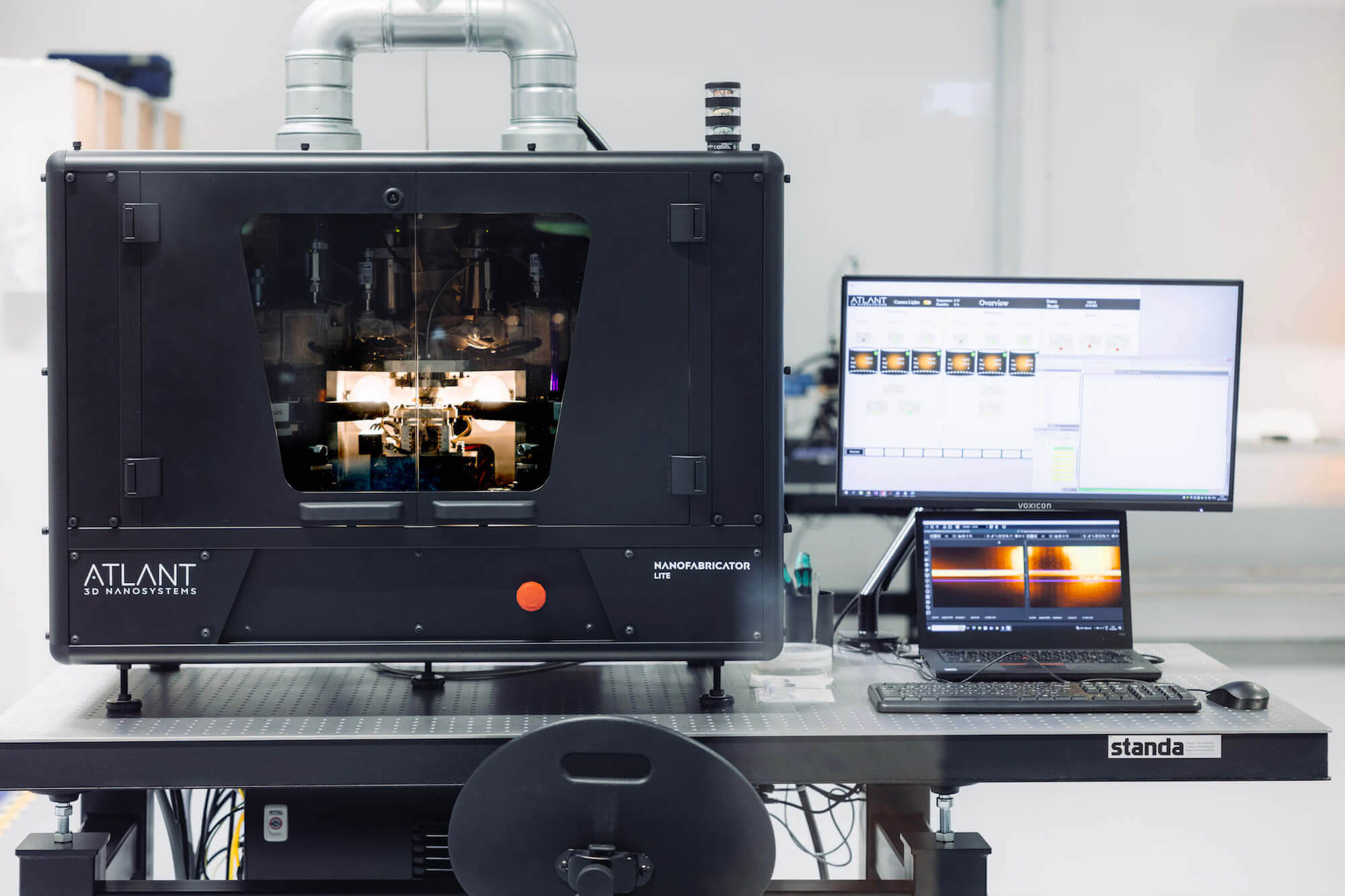
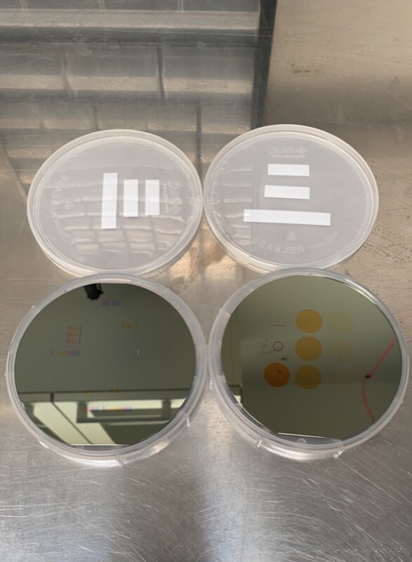
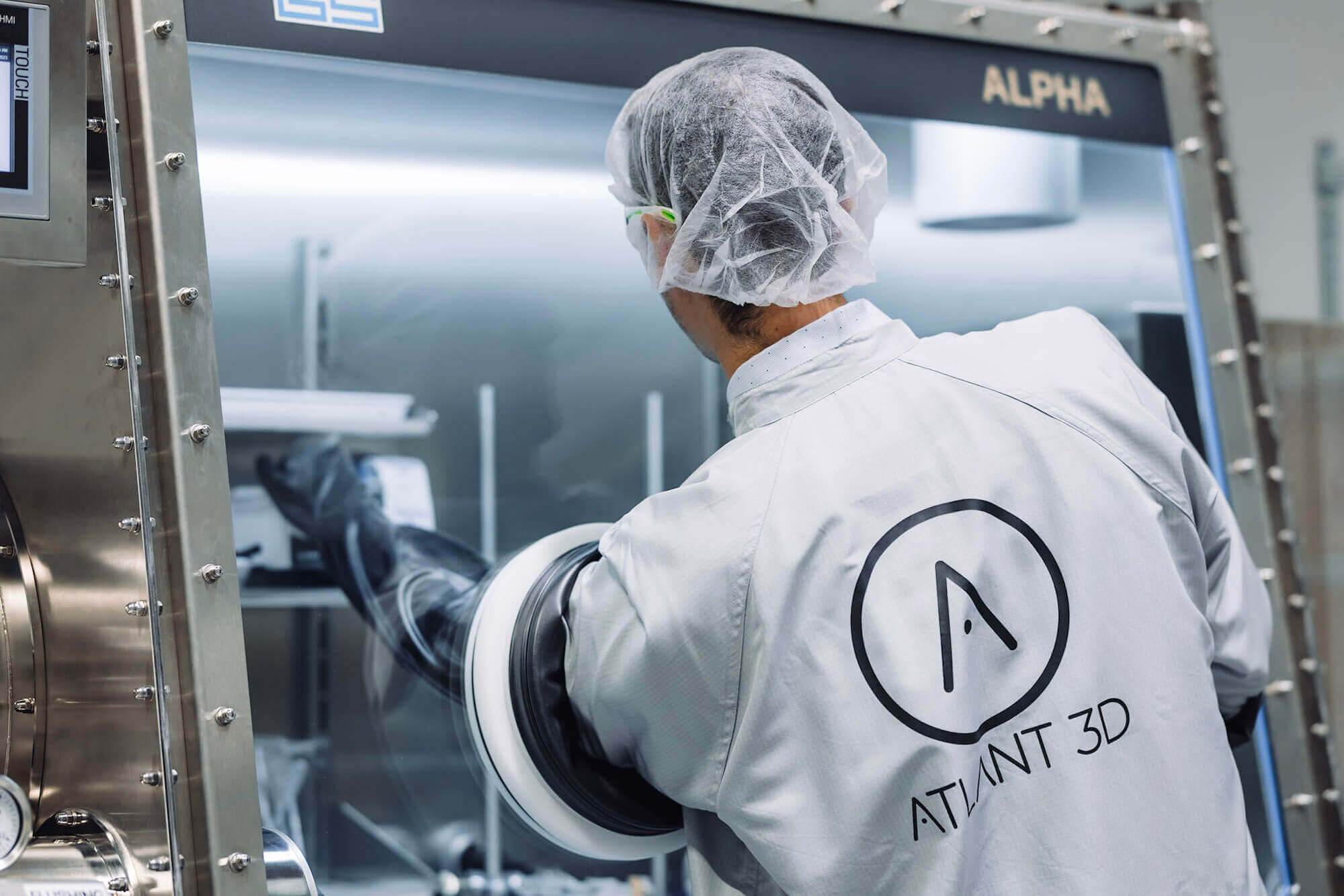
Discover the Future of Micro and Nanofabrication Embark on a journey into the extraordinary world of ATLANT 3D, where groundbreaking innovation meets practical application. We are the architects of the first-ever atomic layer advanced manufacturing platform, reshaping the landscape of advanced materials, microelectronics, and semiconductor solutions. At ATLANT 3D, our mission is to unlock the full potential of nanotechnology. We are dedicated to developing cutting-edge solutions that accelerate innovation, enhance efficiency, and contribute to sustainable practices in the industry. We are building the future atomically precise advanced manufacturing technology & infrastructure for micro and nanoelectronics, optics & photonics on Earth and Beyond. ATLANT 3D is a pioneering atomic scale advanced manufacturing company that utilizes several digital atomically precise processing technologies for enabling rapid innovation across the whole value chain from the investigation of advanced material, prototyping of micro and nanodevices, and scaling manufacturing of final applications in megatrend application domains such as optics, photonics, MEMS/sensors, microfluidics, RF and printed electronics, More than Moore emerging applications, aerospace and defense industries. The current material, devices, and applications innovation cycle in micro/nanoelectronics and functional devices is highly complex and inflexible and requires expensive cleanroom-based infrastructure, including multiple units of expensive equipment and services provided by expensive, highly educated experts. On an innovation level, simple microdevices could be developed within 6-12 months until they are ready for testing. At a global level, such an innovation cycle leads to a globalized supply chain, localized to specific regions and dependent on geopolitical situations. Therefore, many leading countries are in a rush to secure the core of modern industry – semiconductor and electronics manufacturing in their own countries. ATLANT 3D offers a unique technological platform that enables the use of multiple materials, processes, and equipment that will allow on-demand high-precision rapid processing of advanced materials, device prototyping, and manufacturing within hours or days at a fraction of cost comparable to traditional methods and infrastructures. ATLANT 3D offers unique capabilities across the value chain, flexibility in innovation and integration in scalable manufacturing, zero waste, and compatibility with semiconductor industry standards. Moreover, our unique solutions enable creation of zero-waste processes in network-centric innovation ecosystems with Advanced Hubs where innovation cycles is covered from idea to scalable manufacturing and within a fraction of time. We enable the first-ever complete cycle atomic scale advanced manufacturing in a network-centric innovation ecosystem on Earth and Beyond. Direct Atomic Layer Processing (DALP®) represents the core of ATLANT 3D’s innovation. This cutting-edge technology enables unprecedented precision in micro and nanofabrication. DALP® allows for the manipulation of materials at the atomic level, leading to groundbreaking advancements in material science and electronics. Our expertise in atomic layer processing ensures that we can build devices and components with unmatched accuracy and efficiency. DALP® Technology Unlike conventional methods used in microfabrication, DALP® allows for precise atomic layer deposition, etching, and cleaning. This technology enables complex patterning with multiple materials within a single process, which is a considerable advancement over traditional fabrication techniques. Precision and Customization ATLANT 3D’s systems offer unparalleled precision and customization capabilities. They can handle various materials, providing flexibility and precision that is often not achievable with traditional manufacturing technologies. Scalability and Integration ATLANT 3D’s equipment is designed to be scalable and easily integrated into existing manufacturing processes. This makes them a viable option for a range of applications, from small-scale R&D projects to larger industrial manufacturing tasks. The NANOFABRICATOR™ series, encompassing the NANOFABRICATOR™ Lite and NANOFABRICATOR™ Pro, represents our commitment to bringing innovative ideas to fruition. These platforms offer unparalleled versatility in manufacturing, capable of handling over 450 commercially available materials. They are not just tools but enablers of rapid prototyping and production, significantly reducing the time and complexity involved in bringing micro and nanodevices from concept to reality. At ATLANT 3D, we prioritize both versatility and sustainability. Our technology is capable of processing a wide range of materials, offering our partners the freedom to explore and innovate across various applications. Our innovative technology is not just about enhancing existing processes; it’s about creating new possibilities. We are pushing the boundaries of traditional manufacturing, enabling the production of complex structures and devices that were once deemed impossible. Immerse yourself in a cross-disciplinary environment, from design to nanotechnology, and pioneer new knowledge and technologies with us. We cherish the balance between professional dedication and personal well-being, embracing the culture of Danish Hygge and Bavarian-style relaxation. ATLANT 3D’s strategic objective is to radically transform the lifecycle of electronics design and manufacturing. The company’s innovation aims to compress the development timeline from decades to no more than a year, rapidly transforming new ideas into marketable products. This dramatic reduction in time-to-market is a cornerstone of ATLANT 3D’s vision to revolutionize the electronics industry. Central to ATLANT 3D’s vision is the creation of a decentralized, smart advanced manufacturing infrastructure. This infrastructure is grounded in ATLANT 3D’s proprietary know-how and anticipates the integration of other advanced technologies in the future. The establishment of a network of advanced manufacturing hubs, known as A-Hubs, around the globe is pivotal to this vision. These hubs will foster a radical innovation ecosystem, where partners, regardless of their size, can access ATLANT 3D’s technology and knowledge. A-HUB is ATLANT 3D’s premier innovation center, serving as a nexus for collaboration, research, and development in micro and nanotechnology. It is designed to foster partnerships and co-development projects, leveraging our groundbreaking DALP® technology and NANOFABRICATOR machines. A-HUB is where ideas converge, and future technologies are born, offering investors a unique opportunity to be part of pioneering advancements in numerous industries. A-LAB, situated within A-HUB, is our state-of-the-art research and development facility. Here, we conduct pilot projects and joint development initiatives, pushing the boundaries of atomic layer processing and microfabrication. A-LAB represents our commitment to innovation and continuous improvement. A-FAB is an integral part of A-HUB, offering the first-ever on-demand atomic layer advanced manufacturing service. It utilizes our hybrid Microreactor Direct Atomic Processing (μDALP™) to provide customized microfabrication solutions. This service allows clients and partners to experiment, test, and develop new engineering and scientific solutions with unparalleled precision and flexibility. The synergistic operation of A-HUB, A-LAB, and A-FAB underlines ATLANT 3D’s holistic approach to innovation. A-HUB serves as the overarching ecosystem supporting both the R&D-focused A-LAB and the service-oriented A-FAB. This integrated model not only enhances our operational efficiency but also maximizes the impact and reach of our technology. It positions ATLANT 3D as a leader in the micro and nanotechnology sector, offering investors a diversified and robust platform for growth and innovation. Enhanced economic competitiveness & innovation ATLANT 3D’s technology could help countries to develop and manufacture new products and services, enhancing their economic competitiveness. Production of sustainable materials ATLANT 3D’s technology can be used to produce sustainable materials and this could help to reduce the environmental impact of manufacturing. Reduced waste and energy consumption ATLANT 3D’s technology can be used to produce products with less waste and with less energy consumption than traditional manufacturing methods. Our business model focuses on simplifying complex processes, ensuring rapid prototyping and innovation. With a roadmap designed for scalability and adaptability, we are poised for significant growth and technological breakthroughs. Founding: ATLANT 3D was established by three scientists with a vision to enable atomic scale manufacturing. Seed funding: The company secured its initial investment. Team Development: Began building a strong, multidisciplinary team of experts. Pilot Projects: The first pilot project was initiated. Team Expansion: The team grew, underlining the company’s commitment to technological scalability. Intellectual Property: First patent application filed. Collaboration Investment: Secured a collaboration investment with Sony. NASA Project: Signed up for a NASA project. Funding and Team Growth: Continued to expand its team and secured significant funding. EU Projects: Participation in a €10M EU project with partners like Prima Electro & STMicroelectronics, and a €3.6M EU project (ATOPLOT) for developing an industrial pilot system for atomic scale manufacturing. Funding: Raised €15M led by Westhill Capital. NANOFABRICATOR Development: Commenced development of NANOFABRICATOR™ Lite for the Lab/R&D market. NANOFABRICATOR Deployment: Delivered NANOFABRICATOR™ 0G to NASA. Team Expansion: Team size reached 18. Business Model Evolution: The company’s business model transitioned towards LabFab services, NANOFABRICATOR sales, and joint development projects. A-Hub Launch: Launched the first A-Hub in Copenhagen. NANOFABRICATOR Lite Commercialization: Introduced NANOFABRICATOR™ Lite to the market. Team Size: Grew to 30 employees. Geographical and Industry Sector Expansion: Plans for broadening global reach and market penetration. Product Portfolio Diversification: Introducing new models and applications to meet evolving market needs. Strategic Partnerships: Forming essential alliances to enhance market impact and technological influence. Market Dominance: Targeting over €1 billion in revenue, establishing as a leader in atomic-scale manufacturing. Technological Advancements: Continual innovation to maintain market front-runner status. Global Operational Expansion: Setting up additional manufacturing hubs and sales offices worldwide. We understand the importance of informed decision-making for our investors. Our FAQ section addresses key inquiries, providing insights into our strategies, operations, and future prospects.
Investor Relations
![]()
![]()
![]()
![]()
![]()

![]()
![]()
![]()
Shaping the Nano Frontier
 7
PATENT FILED
6
NFL PRE-ORDERED
17
PROJECTS COMPLETED
15
JOIN R&D PROJECTS
7
PATENT FILED
6
NFL PRE-ORDERED
17
PROJECTS COMPLETED
15
JOIN R&D PROJECTS
Redefining Micro and Nanodevice Fabrication
![]() Video insights
Video insights
Exclusive Interview with ATLANT 3D’s investors
![]() FUNDED BY
FUNDED BY
![]() AWARDS & RECOGNITION
AWARDS & RECOGNITION
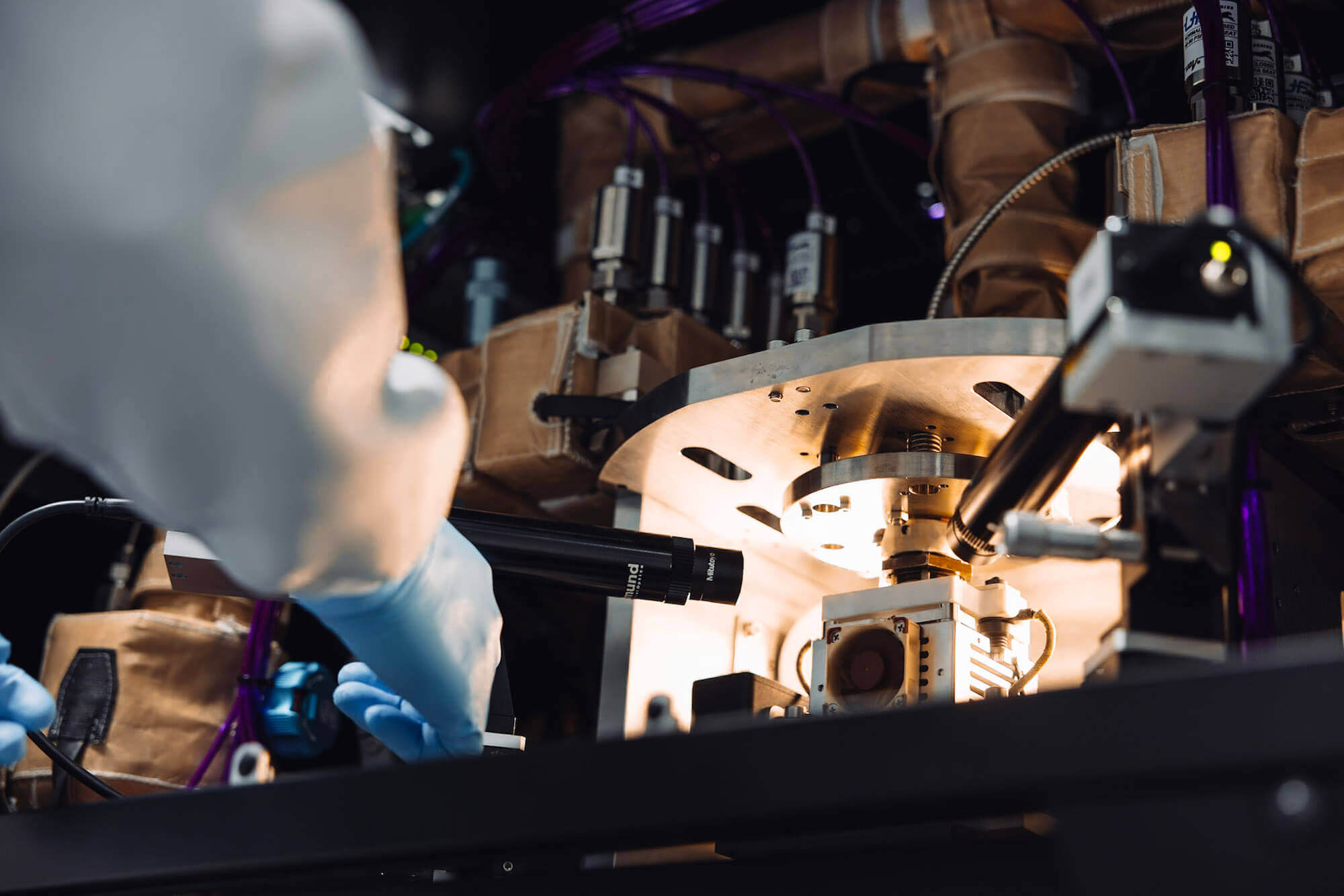
DALP®: Revolutionizing Material Science, The Heart of Our Technological Breakthrough.
OUR SOLUTIONS

Material Versatility and Sustainable Practices
Advancing Beyond Traditional Boundaries
Learning and Development
Work-Life Balance
THE NETWORK-CENTRIC INNOVATION ECOSYSTEM
A-HUB: Driving Collaborative Innovation in Nanotechnology
A-LAB: Pioneering Research and Development
A-FAB: Revolutionizing Manufacturing with Microfabrication as a Service (MaaS)
A Unified Approach to Advancing Micro and Nanotechnology
A Sustainable Approach to Technological Advancement
Sustainability is integral to our mission. We believe that the future of manufacturing must not only be innovative and efficient but also environmentally conscious. Our technologies are designed to reduce waste, lower energy consumption, and minimize the environmental footprint of manufacturing processes. By prioritizing sustainable practices, we aim to lead by example, showing that technological advancement and environmental stewardship can coexist harmoniously.
Microelectronics are essential components in a wide range of products, from consumer electronics to medical devices. However, traditional manufacturing methods for microelectronics are often energy-intensive and produce significant waste. ATLANT 3D offers a new approach to microelectronics manufacturing that is more sustainable and environmentally friendly.


![]() SCALABLE APPROACH
SCALABLE APPROACH
Business Model and Roadmap
2018: Foundational Phase
2019: Early Development and Collaboration
2020: Strategic Partnerships and Funding
2021: Technological Validation and Expansion
2022: Market Introduction and Growth
2023: Scaling and Commercial Launch
2024-2028: Market Penetration and Expansion
2029-2035: Leadership and Global Influence
Questions & Answers
![]() Join Us in Shaping the Future
Join Us in Shaping the Future
We welcome the opportunity to discuss potential partnerships and provide further insights into our company, technology, and investment opportunities.