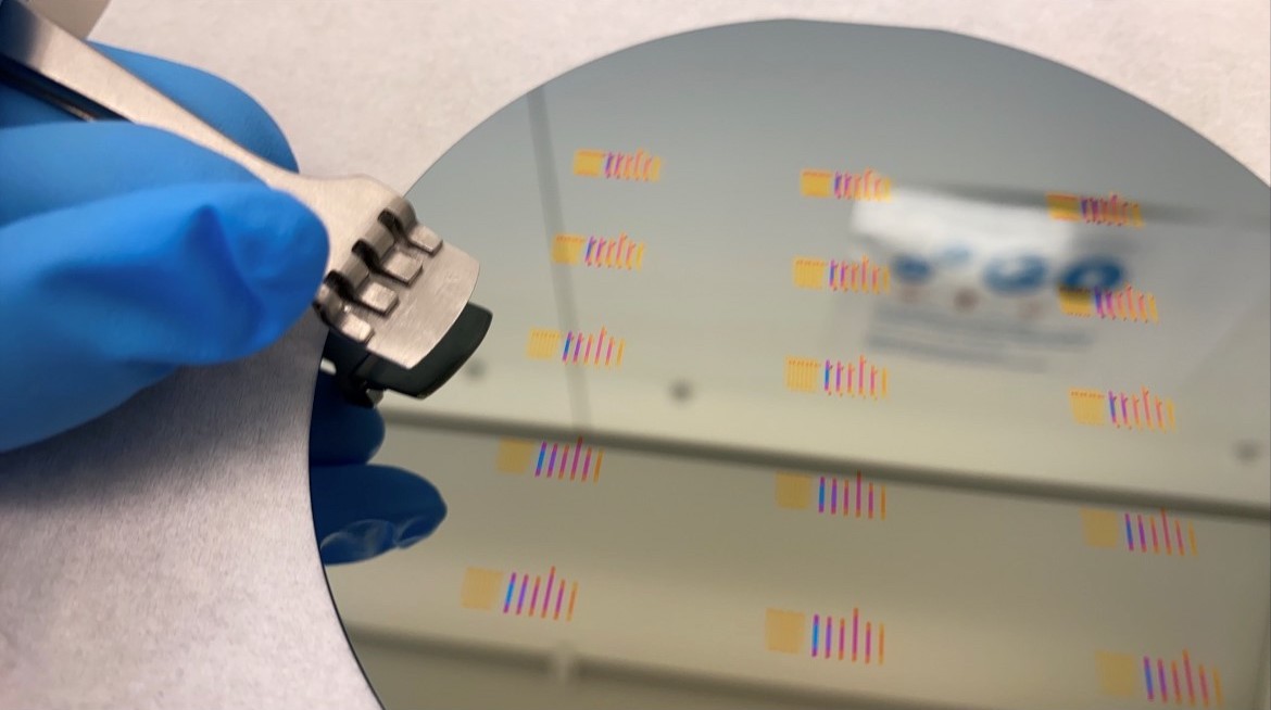
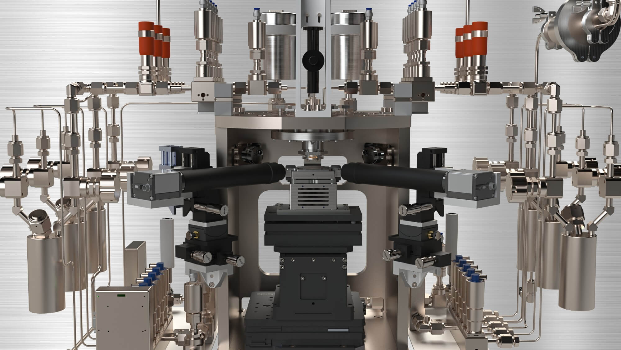
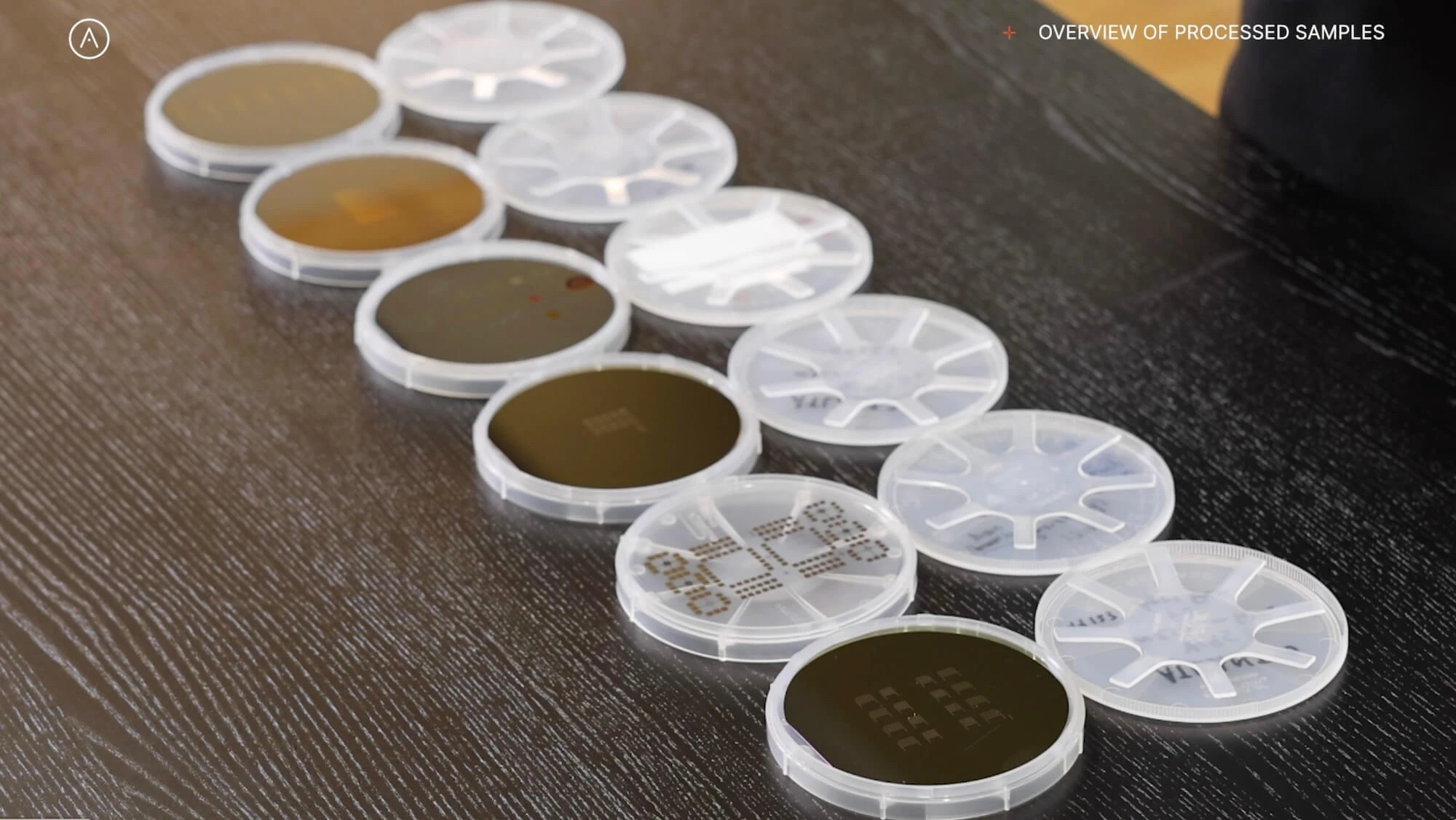
Our technology offers precise, scalable atomic layer manufacturing for rapid creation of micro and nanodevices. Revolutionary technology that enables multi-material, atomically precise, highly scalable atomic layer advanced manufacturing for rapid prototyping and manufacturing of micro and nanodevices. Enabling multi-material deposition in one process, tested on a wide range of advanced materials, independent of surface roughness and substrate sensitivity with multi-shape deposition and a high degree of thickness control. Find out what endless possibilities feel like with our products and services. Trusted by Our patent pending rapid and direct atomic layer processing technology DALP™ offers rapid material and process development and testing, maskless process flexibility, and unparalleled prototyping speed, reducing the time of design iterations, resource allocation and cost of innovation. NANOFABRICATOR™ series enables multi-material deposition in one process, tested on a wide range of advanced materials, independent of surface roughness and substrate sensitivity with multi-shape deposition and a high degree of thickness control. ATLANT 3D is transforming the electronics industry by significantly reducing the time it takes to bring new products to market. Our innovative approach enables us to compress the development timeline from decades to just one year, allowing you to rapidly transform your ideas into marketable products. Discover how ATLANT 3D can support your R&D projects and lab-scale advanced prototyping in our A-HUB facilities, enabling rapid prototyping, pilots and feasibility studies. A-HUB serves as a nexus for collaboration, research, and development in micro and nanotechnology. It is designed to foster partnerships and co-development projects, leveraging our groundbreaking DALP® technology and NANOFABRICATOR machines. A-HUB is where ideas converge, and future technologies are born. Cooperation opportunities: A-LAB, situated within A-HUB, is our state-of-the-art research and development facility. Here, we conduct pilot projects and joint development initiatives, pushing the boundaries of atomic layer processing and microfabrication. A-LAB represents our commitment to innovation and continuous improvement. A-FAB is an integral part of A-HUB, offering the first-ever on-demand atomic layer advanced manufacturing service. It utilizes our hybrid microreactor Direct Atomic Processing (DALP®) to provide customized microfabrication solutions. This service allows clients and partners to experiment, test, and develop new engineering and scientific solutions with unparalleled precision and flexibility. A-HUB serves a broad spectrum of industries, from semiconductor manufacturing to advanced material research, and aerospace to medical technology. Our versatile approach makes A-HUB an ideal partner for sectors that demand the utmost precision and innovation. Engaging with A-HUB opens up a world of possibilities. Whether you’re looking to bring a groundbreaking idea to life or seeking to leverage the latest in atomic layer manufacturing, A-HUB is your gateway. Connect with us to discover how A-HUB can transform your ideas into reality and join the forefront of manufacturing innovation. Solutions
One Technology with Multi-Faceted Process Capabilities for Advanced Manufacturing
![]()
![]()
![]()
![]()
![]()
![]()
![]()
![]()
![]() DALP® Technology
DALP® Technology Rapid, flexible & versatile atomically precise processing

![]() A-HUB
A-HUB ATLANT 3D’s ON-SITE R&D AND MANUFACTURING CAPABILITIES
A-HUB: Driving Collaborative Innovation in Nanotechnology
A-LAB: Pioneering Research and Development
![]() Microfabrication Service
Microfabrication Service A-FAB: Revolutionizing Manufacturing with Microfabrication as a Service (MaaS)
A Diverse Array of Industries at A-HUB


