Expanding Microelectronics Horizons Through Layer Repair & Enhancement
Expanding Microelectronics Horizons Through Layer Repair & Enhancement Even minor imperfections in the material layers of microelectronics can severely impact device performance, yield, and reliability. Traditional fabrication approaches often require costly and time-consuming reworks or complete wafer discards when defects occur. ATLANT 3D’s Direct Atomic Layer Processing (DALP®) technology provides an innovative solution, enabling precise, […]
Accelerating Microfabrication of Semiconductor Devices
Accelerating Microfabrication of Semiconductor Devices Microfabrication processes underpin semiconductor innovation, driving the rapid evolution of electronics and sensor technologies. Yet, traditional microfabrication workflows are often complex, involving multiple steps, extensive manual intervention, and high resource consumption. ATLANT 3D’s Direct Atomic Layer Processing (DALP®) provides a groundbreaking alternative, significantly enhancing fabrication speed, precision, and sustainability through […]
How to Enhance Rapid Prototyping with Atomic Layer Processing
How to Enhance Rapid Prototyping with Atomic Layer Processing Rapid prototyping in microfabrication and electronics lets engineers test, optimize, and iterate without slowing development–accelerating development cycles by orders of magnitude. It drives faster problem-solving and helps new technologies reach users sooner. ATLANT 3D’s Direct Atomic Layer Processing (DALP®) offers a groundbreaking method to elevate rapid […]
Advanced Packaging for Microelectronics Using DALP
Advanced Packaging for Microelectronics Using DALP As chip designs grow more complex, advanced packaging enables shrinking transistors to meet rising performance demands. With traditional scaling nearing its limits, engineers are increasingly turning to heterogeneous integration—stacking and stitching together different technologies inside dense, high-functioning packages. ATLANT 3D’s Direct Atomic Layer Processing (DALP®) provides an exceptional approach […]
An Introduction to Precision Thin Film Deposition with DALP
An Introduction to Precision Thin Film Deposition with DALP Microfabrication continues to broach new limits by shrinking features and fine-tuning materials with atomic control. While techniques like photolithography and ALD deliver high precision, they also demand long, complex workflows. ATLANT 3D’s Direct Atomic Layer Processing (DALP®) changes that equation, bringing atomic-scale accuracy with faster, more […]
Case Study: Precision Deposition of Advanced Materials for Sensor Fabrication
Case Study: Precision Deposition of Advanced Materials for Sensor Fabrication Sensor design keeps raising the bar for precision and integration. As systems shrink and applications grow more complex, microfluidic environments introduce new fabrication hurdles. Among the most difficult is forming reliable conductive electrodes—an essential step that often limits both performance and scalability. ATLANT 3D’s Direct […]
Direct Atomic Layer Processing (DALP®): Unlocking the Future of Atomic-Scale Manufacturing
1: Introduction – Unlocking the Future of Atomic-Scale Manufacturing The field of atomic-scale manufacturing is undergoing a major transformation. As industries demand greater precision, material flexibility, and sustainability, conventional fabrication methods such as Atomic Layer Deposition (ALD), Chemical Vapor Deposition (CVD), and Physical Vapor Deposition (PVD) are reaching their limits. These traditional approaches, while foundational […]
The End of Scarcity: The Nanofabricator is a Machine that Can Make Anything Atom by Atom. Bringing James Burke’s Vision Closer to Reality.
Author: Dr. Maksym Plakhotnyuk, Founder and CEO of ATLANT 3D 1. INTRODUCTION: THE DISAPPEARANCE OF SCARCITY? For centuries, human civilization has been shaped by scarcity – the fundamental economic principle that resources are finite and must be carefully managed. Entire industries, trade systems, and global supply chains are built upon this reality. But what if […]
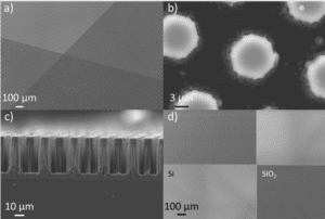
DALP® can deposit multiple materials sequentially in the same chamber to create multilayer structures in a single process step. This capability allows researchers to design prototypes atom by atom, enabling direct patterning and complex designs with arbitrary shapes, with excellent uniformity on complex geometries and sensitive substrates. This user case shows how multi-material device prototypes […]
Our DALP® technology has proven to enabling direct patterning and complex designs with arbitrary shapes, with excellent uniformity on complex geometries and sensitive substrates. It can even process 90° walls and deliver conformal coatings in cavities and around nanostructures with depths up to 60 microns. Additionally, you can control material microstructure from 6 nm nanoparticles […]
ATLANT 3D is proud to introduce our latest whitepaper, "Revolutionizing Prototyping and Design with DALP®." This comprehensive document delves into how our Direct Atomic Layer Processing (DALP®) technology is transforming the landscape of semiconductor manufacturing and prototyping.
ATLANT 3D is proud to introduce our latest whitepaper, "Revolutionizing Prototyping and Design with DALP®." This comprehensive document delves into how our Direct Atomic Layer Processing (DALP®) technology is transforming the landscape of semiconductor manufacturing and prototyping.
Novel approach to patterning in atomic layer deposition
By Matthias Carnoy – Microtechnology Engineer Semiconductor microdevices are nowadays built using a usually long alternating series of additive (vapor deposition, sputtering) and subtractive (dry or wet etching) processes, where patterning is typically defined by photolithography (exposing photosensitive material to UV light through special masks to define a pattern). This manufacturing process needs to be […]
ATLANT 3D technology can be applied on a variety of substrates allowing for a broad range of applications to be possible. One of the advantages is that the technique is applicable on some rough or complex substrates which are sometimes different from patterns using standard lithography techniques. Substrates verified with DALP: Silicon/SiC/GaN wafers. Glass/Fused silica/borosilicates. […]
Interested in learning more? View detailed specifications and features of the Nanofabricator™ Lite. Let’s discuss how Nanofabricator™ Lite can support your unique research goals