Skip links

Industrial R&D

NANOFABRICATOR™ PRO

Empowering material innovation and prototyping with multi-material sequential deposition and unmatched sample versatility levating industrial capabilities. Discover the power of advanced micro- and nano-scale fabrication.

Status

In development

Release Date

August 2024

Sales

Ready for pre-order

Up to 6 Materials simultaneously

400 to 50 µm Line Width

Sample size up to 200 mm

Deposition speed up to 500 mm/s

Sequential deposition of up to 6 materials. 6 different precursors and 6 different reactants can be loaded at the same time, allowing you to quickly switch between the materials you wish to deposit or test.

Samples size up to 200mm. The stage of NANOFABRICATOR™ PRO can accommodate wafers up to 8” and other shapes under 200×200 mm.

Rapid deposition. The NANOFABRICATOR™ PRO stage can move up to 500mm/s, with a deposition speed dependent on the sample and process specifications.

DALP® Technology

The Future of Precision Nanofabrication

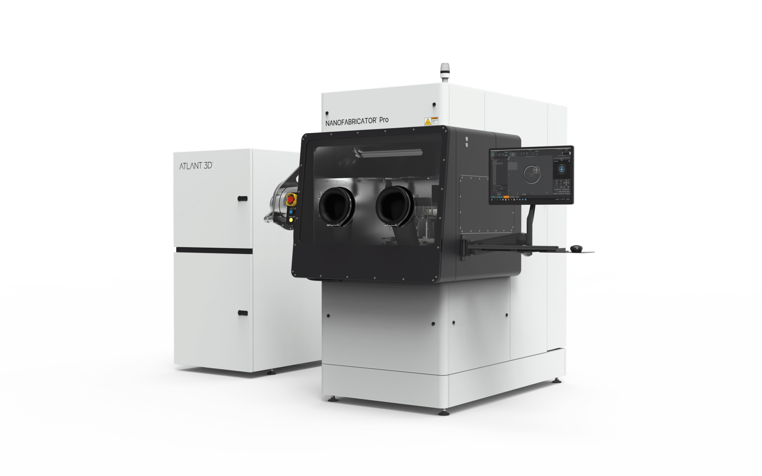
The NANOFABRICATOR™ PRO, ATLANT 3D’s advanced nanofabrication system, is engineered for the future of material innovation. It is a state-of-the-art tool designed for precision and versatility in atomic layer deposition, setting a new benchmark in the field of nanotechnology.

The core of the NANOFABRICATOR™ PRO lies in its revolutionary ability to sequentially deposit up to six different materials. This is achieved through a sophisticated system that simultaneously loads six different precursors and reactants, allowing rapid transitions between materials. The platform’s rapid processing speed, up to 500mm/s, combined with a high-resolution DALP® (micro Direct Atomic Layer Processing) system, ensures precise and efficient material deposition.

WATCH VIDEO

PARADIGM SHIFTING PROCESS

ATLANT 3D’s proprietary DALP® – DIRECT ATOMIC LAYER PROCESSING technology is enabling a paradigm shift across the whole value chain from advanced material innovation to advanced manufacturing of industrial solutions.

CURRENT PROCESS
Current photolithography-based process
ATLANT 3D’s DALP®
Direct Atomic Layer Processing​
BENEFITS

Key features of the NANOFABRICATOR™ PRO

The NANOFABRICATOR™ PRO offers a suite of benefits that transform the way materials are developed and devices are crafted. Whether it’s for cutting-edge research or groundbreaking industrial applications, the NANOFABRICATOR™ PRO opens doors of innovation.

  • Versatility: Accommodates a wide range of materials and sample sizes up to 300×300 mm.
  • Precision: Advanced DALP® technology offers exceptional control over deposition with resolutions up to 400 μm.
  • Efficiency: High-speed deposition capabilities significantly reduce processing time.
  • Adaptability: Manual loading and vacuum holding methods provide flexibility for various research needs.
  • Consistency: Maintains high uniformity in heater temperature crucial for sensitive processes.
Advanced Microfabrication

RAPID, FLEXIBLE, VERSATILE & ATOMICALLY PRECISE PROCESSING

At the heart of the NANOFABRICATOR™ PRO is the Direct Atomic Layer Processing (DALP®) technology, a breakthrough in nanoscale engineering. This technology allows for atomic-scale precision, enabling the creation of materials and devices with unprecedented accuracy and complexity.

It is designed for rapid prototyping and the development of new device structures, offering a wide selection of materials for Atomic Layer Deposition (ALD) processes. Additionally, its lithography-less single-wafer optimization significantly streamlines the fabrication process, making it an ideal tool for innovative and efficient prototype development in various scientific and industrial fields.
DALP® has revolutionized prototyping, turning a traditionally lengthy process into a rapid, precise operation. Key benefits include accelerated development cycles, atomic-level control for complex prototypes, versatile material and surface adaptability, and cost reductions due to increased efficiency. This advancement in DALP® fosters a conducive environment for innovative microdevice fabrication, marking a significant leap in microfabrication technology.

Innovation

+50%

Efficiency

10x

Materials

450+

Research and Development Capabilities

Our patent pending rapid and direct atomic layer processing technology DALP® offers rapid material and process development and testing, maskless process flexibility, and unparalleled prototyping speed, reducing the time of design iterations, resource allocation and cost of innovation. ​

The NANOFABRICATOR™ PRO is a researcher’s ally, providing unmatched capabilities for innovative research and development in nanotechnology. Its ability to handle diverse materials and complex deposition processes makes it ideal for experimental and pioneering work in advanced material science.

Line Width

100 µm now, 25 µm in development, 1 µm long term goal

Temperature

Operates in a temperature range from room temperature (RT) up to 300°C

Process speed

Variable from 0.1 mm/s up to 500 mm/s (based on sample and process specifications).

Versatile Materials Platform

Possible to process several materials sequentially out of 150* possible.

Environment

Inert (argon-recommended) or within controlled ambient environments

Hybrid processing

Direct additive and subtractive processing

Selective Area Deposition

Path-defined processing for targeted deposition of materials

Surface geometry

Conformal deposition on any type of surface with corrugation up to 25 µm

Multimaterial stack printing

Multiple materials can be deposited sequentially

Crystalline Material

Growth High quality material deposition

Selective nanoparticle deposition

Tested with platinum (Pt) processes

Hollow microstructuring

Post process hollow structure development

PROCESS INNOVATION INSIGHTS

DALP® represents a quantum leap in process innovation, encapsulating direct patterning with remarkable process flexibility. It advances the understanding of material deposition, addressing the complexities of cross-sectional line profiles and the intrinsic nature of atomic growth. The DALP® excels in the deposition on intricately contoured surfaces, negating the necessity for vacuum environments — thereby streamlining the manufacturing workflow and enhancing the efficiency of material innovation.

SURFACE STRUCTURATION

Staircase with 0.3 nm step height and 3 microns step width.

Smooth 1.5 nm height valleys repeated.

Tapered shape structure.

Cross-sectional line profile and growth nature

Characterization of self-limiting surface chemistry and digital growth in DALP®. Thicknesses are determined for two distinct DALP® materials by ellipsometry.

CONFORMALITY

Cross-section of platinum deposition for capacitive sensor in the 20 µm channel. The EDX scans shown to the right indicate conformal deposition of platinum along the sidewalls.

Direct patterning & process flexibility

The DALP® system demonstrates its capacity to engineer patterns with atomic precision, facilitating the creation of complex microscale structures.

SUBSTRATE VERSATILITY

ALD conformality and low T. deposition enables processing sensitive and rough substrates. Silicon/SiC/GaN wafers. Glass/Fused silica/borosilicates. Polymer.

CONFORMALITY

A. “Anodic” aluminum oxide macropores coated with Pt. B. Nanostructured black Si surface coated Pt different thickness. C. Si trench coated with a Pt carbon nanograss. D. Aligned Si trenches coated with a perpendicular line of TiO2

 Sustainability

Setting New Benchmarks in Sustainable Manufacturing

At ATLANT 3D, we are not just changing how things are made; we are redefining the principles of manufacturing. Our commitment to sustainability is a testament to our belief that responsible innovation and business practices can create a positive impact on the world, paving the way for a more sustainable future in manufacturing and beyond.

Learn more
Nanofabricator™ PRO

Technical Specification

Substrate

  • Size: up to 8″ (200mm)
  • Substrate Handling​: Wafer
  • Maximum thickness: 10 mm
  • Z direction shape: Flat
  • Holding method: Vacuum
  • Loading: Manual
  • Heater temperature: max. 300°C
  • Heater temp. uniformity: +/- 0.5%

Process Chamber

  • Environment: Inert***** Controlled​
  • Processing speed****: up to 500mm/sec
  • Deposition area: up to 1.5mm from wafer edge
  • DALP® resolution: 100 μm standard
  • Precursor temperature: RT – 150°C
  • Nr. of precursor bubblers: 2**
  • Nr. of reactant bubblers: 1** (H2O***)
  • Nr. of gas reactants: 1**

Options

  • Additional precursor bubblers: **
  • Additional reactant bubblers: **
  • Additional gas reactants: **

* Dependent on materials to be deposited and customer needs.

** Additional number of bubblers and reactants dependent on customer needs

***** Argon recommended.

*** Additional reactant types dependent on customer needs.

**** Clean room, CLASS 8 min recommended.

Questions & Answers

The NANOFABRICATOR™ PRO, a flagship product from ATLANT 3D, represents a significant leap in advanced material innovation and nanofabrication technology. Designed to accommodate a diverse range of materials and sample sizes, it offers unparalleled flexibility and precision in atomic layer deposition.

DALP®, or Microreactor Direct Atomic Processing, is a hybrid technology enabling on-demand atomic layer manufacturing. It allows for precise printing of microdevices on various surfaces, offering functionality and speed at a reduced cost​​.

It’s ideal for applications in MEMS & Sensors, Optics, Photonics & Novel Displays, Advanced Packaging, RF & Microelectronics, and Emerging Applications.

Yes, it incorporates both Temporal ALD, which involves sequential pulse sequences for precursor and co-reagent delivery, and Spatial ALD, which offers spatial separation of these elements with increased deposition speed.

Yes, it is capable of processing on diverse substrates like Silicon/SiC/GaN Wafers, Polymers, Glass, Fused Silica, and Borosilicates.

Yes, the NANOFABRICATOR™ PRO is designed to be flexible and can be adapted to specific project requirements.

The system offers atomic scale thickness variability and precise gradient control for accurate material deposition.

It is designed to seamlessly integrate into lab infrastructures.

ATLANT 3D offers comprehensive support for the NANOFABRICATOR™ PRO, including training and technical assistance.

Capabilities

The NANOFABRICATOR™ PRO equipped to handle sequential deposition of up to six materials with rapid switching capabilities, the NANOFABRICATOR™ PRO can support sample sizes up to 200×200 mm and wafers up to 8 inches. Its advanced features, such as a high-speed stage capable of moving up to 500mm/s and a finely-tuned heating system with exceptional temperature uniformity, make it an ideal tool for cutting-edge research and development in microelectronics, photonics, and beyond.

The NANOFABRICATOR™ PRO excels in rapid material testing, enabling precise exploration of new materials and swift development of innovative processes, crucial for cutting-edge research and development.

It facilitates the development of complex device structures by allowing multi-material deposition in a single process. This feature is vital for industries like semiconductor manufacturing and photonics, where intricate device architectures are commonplace.

Yes, it is equipped to handle a variety of precursor gases, essential for diverse material processing. This versatility is key in experimenting with new material combinations and properties.

The NANOFABRICATOR™ PRO supports sequential up to 6 materials simultaneously. It is equipped to load six different precursors and six different reactants simultaneously, enabling quick transitions between various materials for deposition or testing.

The NANOFABRICATOR™ PRO can accommodate wafers up to 8 inches (200×200 mm), as well as other shapes within these dimensions.

The deposition speed is dependent on the sample and process specifications. The stage can move up to 500mm/s, offering rapid deposition capabilities.

The NANOFABRICATOR™ PRO is designed for wafers ranging in size from 2 inches to 8 inches, with a maximum thickness of 10 mm. The Z-direction shape of the wafers should be flat.

Samples are held in place through a vacuum holding method, ensuring stability during the deposition process.

It features a heater with a maximum temperature of 300°C. The heater temperature uniformity is maintained within +/- 0.5% to ensure consistent processing conditions.

It offers a DALP® resolution of 100 μm, allowing for detailed and precise deposition.

Yes, it is capable of handling wafers up to 200mm (8 inches) in diameter.

Operations & Control

The NANOFABRICATOR™ PRO is sophisticated system sets a new standard in nanoscale engineering, embodying ATLANT 3D’s commitment to pioneering innovations in the realm of atomic-scale manufacturing.

The NANOFABRICATOR™ PRO operates with proprietary software designed to control its advanced features and functionalities.

The integrated software is essential for optimizing the deposition processes, enabling precise control over parameters such as material flow, deposition rates, and layer thickness. It may also include analytical tools for process evaluation and improvement.

The system could be configured for remote monitoring and possibly control, depending on user requirements and security considerations.

Emerging applications like quantum computing, advanced sensors, and next-generation energy storage technologies can significantly benefit from the precision and versatility offered by the NANOFABRICATOR™ PRO.

The ability to operate in an ambient environment allows for more flexible and practical integration into various research and production settings, reducing the need for specialized controlled environments.

Absolutely, its design caters to both R&D labs and production lines, offering flexibility in scaling from prototype development to full-scale production.

We are providing ongoing support, including operational training, technical assistance, and maintenance services, ensuring customers can fully leverage the capabilities of the NANOFABRICATOR™ PRO.

ATLANT 3D
ATLANT 3D
Explore
Drag