

An Introduction to Precision Thin Film Deposition with DALP
Microfabrication continues to broach new limits by shrinking features and fine-tuning materials with atomic control. While techniques like photolithography and ALD deliver high precision, they also demand long, complex workflows. ATLANT 3D’s Direct Atomic Layer Processing (DALP®) changes that equation, bringing atomic-scale accuracy with faster, more flexible processing.
Understanding DALP®
DALP® represents a fundamental shift from conventional thin-film techniques. Unlike traditional ALD, which deposits materials uniformly across an entire substrate, DALP® achieves selective deposition directly onto target areas. This precise patterning is enabled by a micro ALD reactor nozzle, which delivers reactive precursors locally, performing atomic layer deposition exactly where required.
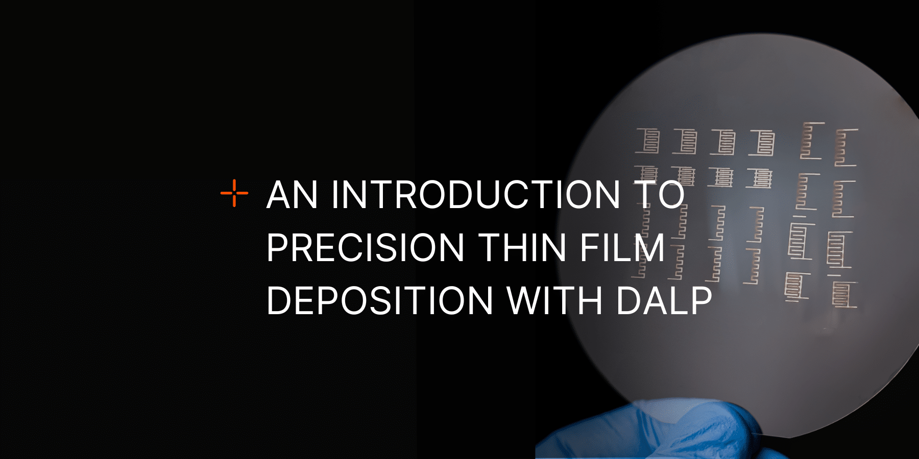
The essence of DALP® is the targeted, layer-by-layer material deposition, driven entirely by digital designs. Engineers can simply convert their CAD designs directly into deposition patterns without the need of physical masks. This maskless approach dramatically reduces the steps involved, simplifying fabrication processes while improving precision and reproducibility.
DALP® vs Traditional Techniques
Conventional microfabrication often demands extensive use of photomasks, resists, and multi-stage processing (e.g., etching and lift-off). In contrast, DALP® completely bypasses these processes. It directly deposits atomic layers precisely and exclusively onto predefined regions of a substrate, drastically cutting down fabrication complexity and enhancing throughput.
DALP® further surpasses other contemporary methods like inkjet or aerosol jet printing, which lack the precise thickness control at the nanoscale. DALP® achieves precise vertical resolution, routinely handling film thickness increments as small as 0.3 nm—a feat extremely challenging and time-consuming to accomplish with conventional processes.
Unique Capabilities and Applications
DALP® opens new possibilities in microfabrication, including creating intricate 2D geometries, precise multidirectional thickness gradients, and sophisticated overlapping multi-material patterns in a streamlined workflow. For example, a gradient or stepped thin film typically requiring multiple conventional processes can be executed in one DALP® run, saving considerable time and resources.
The technology’s adaptability to a wide variety of standard ALD chemistries ensures a broad material palette, encompassing metals, oxides, nitrides, and more. Consequently, DALP® effectively prototypes advanced microelectronic, photonic, and sensor structures with complexity previously deemed impractical.
Key application examples include:
- Surface patterning for optical property control and wettability adjustments.
- Miniaturized Bragg mirror structures for photonics.
- Thin-film capacitors and integrated sensor devices.
- Precision encapsulation and functionalized microstructures.
Transforming the Microfabrication Industry
Beyond its immediate technical advantages, DALP® holds profound implications for semiconductor innovation and agile prototyping. By reducing the design-to-fabrication cycle from weeks or months to mere hours, DALP® fundamentally transforms the pace of microdevice development. Its streamlined nature enables researchers and engineers to rapidly iterate designs and quickly validate new ideas.
Moreover, DALP® democratizes high-precision microfabrication. It lowers entry barriers, allowing institutions without extensive cleanroom facilities to undertake ambitious research and prototyping projects. This accessibility accelerates innovation across diverse applications such as quantum computing, advanced sensors, MEMS, and custom electronic components.
Looking forward, DALP® may integrate deeply with existing fabrication lines or even reshape parts of traditional semiconductor manufacturing workflows. Its ability to precisely deposit atomic layers on demand, coupled with digital-driven flexibility, aligns well with future trends towards personalized and sustainable microfabrication.
Conclusion
ATLANT 3D’s DALP® technology represents a revolutionary leap in atomic-scale processing. By directly merging atomic precision with additive manufacturing principles, DALP® delivers unmatched flexibility, efficiency, and innovation potential to microfabrication. This unique combination not only simplifies existing workflows but also sets a new standard for future semiconductor and microelectronics research, promising to transform how next-generation devices are imagined, developed, and produced.
An Introduction to Precision Thin Film Deposition with DALP Information
DATE:
LOCATION: