


Our DALP® technology has proven to enabling direct patterning and complex designs with arbitrary shapes, with excellent uniformity on complex geometries and sensitive substrates. It can even process 90° walls and deliver conformal coatings in cavities and around nanostructures with depths up to 60 microns. Additionally, you can control material microstructure from 6 nm nanoparticles to 1 cm fully dense, pinhole-free layers, including nanoporous layers.
CONFORMALITY
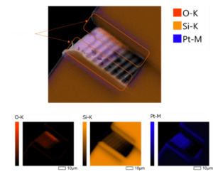
- Cross-section of platinum deposition for capacitive sensor in the 20 µm channel. The EDX scans shown to the right indicate conformal deposition of platinum along the sidewalls.
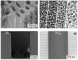
(a) Anodized aluminum oxide macropores coated with Pt: the roughness of Pt nuclei is clearly visible and homogeneous along the pore length.
(b) Nanostructured black Si surface coated with 20/300/600/1000 DALP® Pt passes.
(d) Low-magnification SEM of a TiO2 line in top view on a Si substrate structured with trenches.
(c) High-magnification of the Pt layer presented in cross-section inside a Si trench.
It is proven to achieve smooth conformal deposition on complex surfaces like “Anodic” aluminum oxide macropores, nanostructured black Si surfaces, Si trenches, and aligned Si trenches with a surface roughness of up to 25 µm.
ALIGNMENT PRECISION
- Possible to deposit alignment marks on the sample
- Alignment process in development right now
- Expected accuracy ~1 μm
DEPOSITION PRECISION
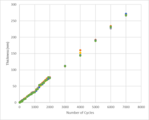
- Linear increase in thickness with the number of cycles
- Growth rate is dependent on the material
- Deviation of 8% at 10 nm and 1% at 270 nm
- Deviation of 4% after 3 months
DEPOSITION UNIFORMITY
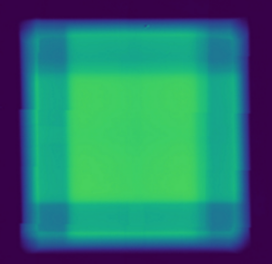
- High degree of uniformity within the central area
- Typically better than 1%
Precision, Uniformity and Conformality Information
DATE:
LOCATION: