

Direct Atomic Layer Processing (DALP) is an advanced nanomanufacturing technique that extends conventional Atomic Layer Deposition (ALD) and Atomic Layer Etching (ALE) by enabling site-specific, localized material processing at the nanoscale. Unlike traditional methods that apply materials uniformly across entire substrates, DALP enables localized deposition and etching in specific areas, potentially reducing the need for additional patterning steps and enhancing fabrication efficiency.
Background
Atomic Layer Deposition (ALD) and Atomic Layer Etching (ALE) are widely used techniques in nanofabrication, known for their ability to deposit or remove material with atomic-level precision. However, traditional methods often require masks and post-processing steps to achieve localized features, which increases complexity and cost. DALP addresses these limitations by providing direct spatial control over the deposition and etching processes, allowing for precise material placement without the need for masks or additional lithographic steps.
DALP was developed to address challenges in nanofabrication, particularly in advanced electronics, photonics, and nanotechnology. Its localized processing capability makes it suitable for applications where conventional techniques face challenges, such as on flexible substrates or in areas with complex geometries.
Technology Overview
DALP operates by spatially separating chemical precursors and reactants, which are delivered independently to specific locations on a substrate using micro-nozzle systems. This ensures that chemical reactions occur only within targeted zones, reducing cross-contamination and enhancing precision. The process achieves micrometer-scale lateral resolution and nanometer-scale vertical precision.
Material growth or etching occurs as the nozzle moves across the substrate, allowing real-time patterning without the need for traditional masking or post-lithography steps. This approach offers several advantages, including localized processing, scalability for industrial applications, and compatibility with various materials such as metals, oxides, and semiconductors.
Key Features
- Localized Deposition and Etching: DALP is capable of processing materials on substrates that may be challenging for traditional lithographic techniques, such as polymers and flexible films.
- Gradient and Multi-Thickness Patterns: By controlling the movement of the micro-nozzle in the XY plane, DALP can create gradient structures and multi-thickness patterns, which are useful in devices requiring spatially varying material properties.
- Rapid Prototyping: The maskless nature of DALP allows for fast prototyping of devices, significantly reducing fabrication time.
Applications
DALP has broad applications across various scientific and industrial domains, including:
- Semiconductor fabrication: Enables highly localized deposition for thin-film transistor devices. [1]
- Optical devices: Allows precise gradient control of thickness and refractive index in thin-film optical components and metasurfaces. [2]
- MEMS and photovoltaic devices: Facilitates surface passivation and encapsulation for devices with complex substrate geometries. [3]
- Sensor technology: Used in fabricating advanced gas sensors, microfluidic sensors, and thin-film metal pressure and temperature sensors. [4][5]
Development and Research Contributions
The development of DALP has been a collaborative effort involving multiple academic and industrial institutions. Notable contributions include:
- Dr. Maksym Plakhotnyuk (Technical University of Denmark), Ivan Kundrata (Slovak Academy of Sciences), and Dr. Julien Bachmann (Friedrich-Alexander-Universität Erlangen-Nürnberg): Their joint research on localized deposition techniques culminated in the publication “Additive Manufacturing in Atomic Layer Processing Mode.” [6]
- University of Grenoble and University of Lyon: Dr. David Muñoz-Rojas (Grenoble) worked on enhancing spatial ALD techniques, while Dr. Catherine Marichy (Lyon) contributed to direct surface structuration and maskless deposition methods. Their efforts contributed to advances in the scalability and precision of localized ALD processes. Demonstrations and Case Studies
Several studies have demonstrated the capabilities of DALP in producing films with high crystallinity and chemical purity. Examples include:
- Deposition of TiO2 and platinum lines: These experiments illustrated DALP’s ability to achieve uniform thickness and high-resolution patterns.
- Gradient deposition: Demonstrated the process’s capability in creating gradient structures for advanced device architectures.
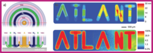
(a) Schematic of a micro-nozzle used in Direct Atomic Layer Processing (DALP), showing the spatial separation of precursors and reactants. (b) Example of localized deposition demonstrating nanoscale thickness control and uniformity. (provided by ATLANT 3D)
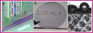
(a) Schematic representation of localized ALD using spatial control of precursors and reactants. (b) Example of a patterned substrate with “LOC ALD” created using localized atomic layer deposition. (c) Images demonstrating surface wettability modification, showing different contact angles before and after deposition [3]. (provided by Marichy et al., “Direct surface structuration and functionalization using localized Atomic Layer Deposition”)
References
- Stefanovic, Sonja, et al. “Direct‐Patterning ZnO Deposition by Atomic‐Layer Additive Manufacturing Using a Safe and Economical Precursor.” Small 19.36 (2023): 2301774.
- Plakhotnyuk, Maksym, et al. “Advanced Optical Control through Atomic Layer Surface Engineering.” Novel Patterning Technologies 2024. SPIE, 2024.
- Plakhotnyuk, Maksym, et al. “Inherently Selective Atomic Layer Deposition for Optical and Sensor Applications: Microreactor Direct Atomic Layer Processing (μDALP™).” Electrochemical Society Meeting Abstracts 244. No. 29. The Electrochemical Society, Inc., 2023.
- Barr, Maissa KS, et al. “Fabrication of Free-Standing Three-Dimensional Structures By Atomic Layer 3D Printing.” Electrochemical Society Meeting Abstracts 240. No. 29. The Electrochemical Society, Inc., 2021.
- Hudec, Boris, et al. “Demonstration of Resistive Pt Temperature Sensors Directly Printed Using Novel Atomic-Layer 3D Printer.” Electrochemical Society Meeting Abstracts 240. No. 55. The Electrochemical Society, Inc., 2021.
- Kundrata, Ivan, et al. “Additive Manufacturing in Atomic Layer Processing Mode.” Small Methods 6.5 (2022): 2101546.
- Munoz-Rojas, David, et al. “Speeding up the unique assets of atomic layer deposition.” Materials Today Chemistry 12 (2019): 96-120.
- Marichy, Catherine, et al. “Direct surface structuration and functionalization using localized Atomic Layer Deposition.” Trends in NanoTechnology 2023. 2023. Stefanovic, Sonja, et al. “Direct‐Patterning ZnO Deposition by Atomic‐Layer Additive Manufacturing Using a Safe and Economical Precursor.” Small 19.36 (2023): 2301774.
DALP®WIKI Information
DATE:
LOCATION: