

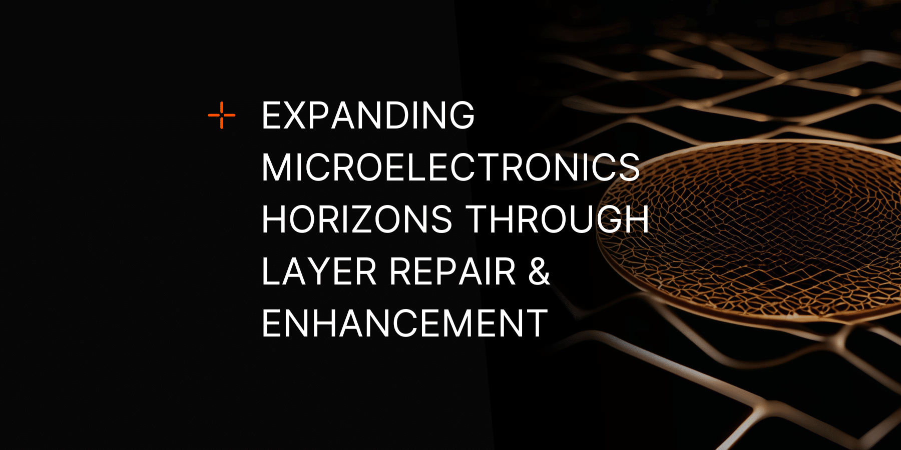
Expanding Microelectronics Horizons Through Layer Repair & Enhancement
Even minor imperfections in the material layers of microelectronics can severely impact device performance, yield, and reliability. Traditional fabrication approaches often require costly and time-consuming reworks or complete wafer discards when defects occur. ATLANT 3D’s Direct Atomic Layer Processing (DALP®) technology provides an innovative solution, enabling precise, localized repairs and enhancements directly during the fabrication process—transforming microelectronics manufacturing into an agile and adaptive workflow.
DALP® for In-Process Corrections
DALP®’s capability to perform precise, localized material deposition offers pioneering in-process correction possibilities. Unlike traditional methods that are rigid and purely subtractive, DALP® can deposit additional material exactly where needed to correct defects seamlessly. This targeted approach prevents unnecessary reworks or wafer disposal, significantly enhancing manufacturing yield and device reliability.
Insulating Layer Repairs
One common issue in semiconductor manufacturing is defects in insulating layers, which can cause short circuits or functional impairments. Traditional correction methods often prove impractical, especially once subsequent layers cover these areas.
DALP®, however, can precisely reapply insulating materials, such as silicon dioxide or polymer films, directly onto identified defect sites. Through accurate deposition, DALP® restores the integrity of insulating films without disrupting surrounding structures, dramatically reducing the need for comprehensive reprocessing and increasing manufacturing efficiency.
Optical Coating Adjustments
Optical coatings, critical to photonic devices, sensors, and lithographic processes, require precise thicknesses to meet exact optical specifications. Traditional processes struggle to adjust thickness post-deposition, often requiring complete reworks.
DALP® uniquely solves this challenge by enabling incremental, atomic-level thickness adjustments post-inspection. If a coating is slightly under or over specification, DALP® precisely adds material layers as necessary to fine-tune optical properties, ensuring compliance with stringent optical performance requirements without restarting the deposition cycle.
Dielectric Layer Enhancements
Dielectric layers are fundamental in semiconductor devices, affecting performance attributes such as capacitance, isolation, and breakdown voltage. Minor defects or non-uniformities in dielectric films can significantly impact device performance.
DALP® enables engineers to precisely correct and enhance dielectric layers during fabrication. By selectively reinforcing thin or compromised regions with targeted deposition, DALP® ensures uniform dielectric properties across the entire device surface, enhancing overall reliability and device performance consistency.
Yield Improvement and Rework Reduction
The targeted corrective capabilities of DALP® significantly enhance manufacturing yield by addressing defects immediately upon identification. By repairing layer defects precisely and locally, DALP® substantially reduces the need for complete wafer discards or extensive reworks, resulting in notable cost savings and improved throughput.
Yield losses and rework activities directly affect the economics of microelectronics manufacturing; DALP®’s adaptive in-process corrections mitigate these costs, directly enhancing profitability and production efficiency.
Sustainability and Resource Efficiency
DALP®’s precision deposition technology not only reduces operational complexity but also significantly contributes to sustainable manufacturing practices. By minimizing material waste and chemical usage through targeted corrections, DALP® dramatically lowers environmental impact compared to traditional processes.
Reducing material consumption and rework frequency conserves valuable resources and reduces energy consumption, aligning semiconductor manufacturing with global sustainability initiatives and environmentally responsible production practices.
Conclusion
ATLANT 3D’s DALP® technology sets a new standard for microelectronics manufacturing, transforming rigid, defect-prone processes into flexible, adaptive workflows. Through precise in-process layer repair and enhancement capabilities, DALP® dramatically increases yield, reduces rework and scrap, enhances device reliability, and promotes sustainability. By empowering manufacturers with atomic-level precision and real-time adaptability, DALP® paves the way for the future of microelectronics—where innovation, efficiency, and sustainability converge seamlessly.
Expanding Microelectronics Horizons Through Layer Repair & Enhancement Information
DATE:
LOCATION: