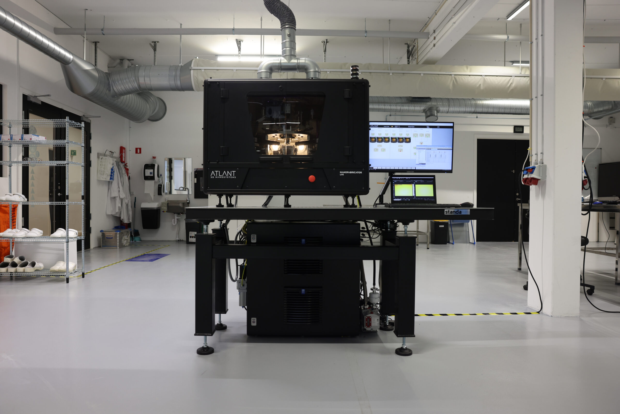
Scientists and engineers working at the boundaries of light manipulation face a fundamental challenge: bridging the gap between theoretical potential and physical implementation. By enabling direct atomic-layer processing of optical materials, new approaches to device architecture become possible. High-index optical components Anti-reflective and UV applications Reflective surfaces Active optical elements Photovoltaic structures Fused silica, Borosilicates Full-spectrum transmission characterization Our team has validated multiple optical and photonic implementations: Optics & Photonics
Optics & Photonics
Atomic-Scale Control for Optical & Photonic Systems
Beyond the Boundaries
of Traditional Processing Shape Optical
Properties
Advance Photonic
Integration
Process Parameters


Material Systems

Platform Compatibility


Research Outcomes
Validated hyperspectral imaging filters with
Direct CMOS sensor integration
Quantified optical performance metrics Demonstrated multi-layer Bragg structures with controlled interfaces

Explore Applications

Nik Thorsen
Business Development Manager

