

ATLANT 3D is proud to introduce our latest whitepaper, “Revolutionizing Prototyping and Design with DALP®.” This comprehensive document delves into how our Direct Atomic Layer Processing (DALP®) technology is transforming the landscape of semiconductor manufacturing and prototyping.
The Power of DALP® Technology
Speed and Efficiency DALP® technology significantly reduces the time required to go from concept to prototype. Traditional methods often involve extensive time and numerous processing steps. In contrast, DALP® allows for the creation of complex designs and varying thickness gradients in just hours. From initial design to the start of processing, the entire procedure takes approximately 2-3 hours, with the machine’s operational time being around 24 hours and minimal manual intervention.
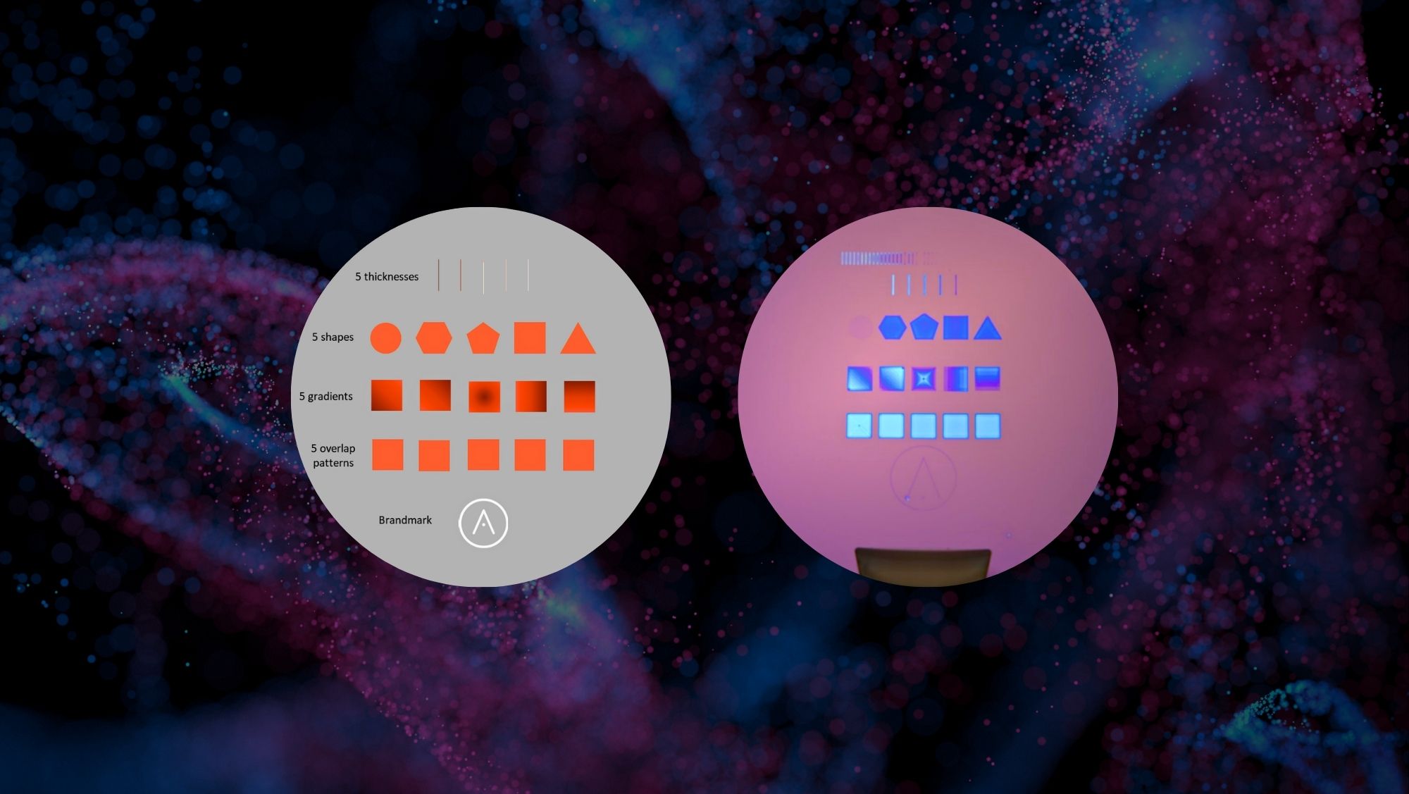
Material Flexibility With DALP®, you can achieve a wide range of designs, including various 2D shapes, multidirectional thickness gradients, and complex overlapping patterns. The technology supports a diverse array of materials, providing customization options previously unavailable in the industry. For instance, our sample wafer using TiO2 on a 4-inch Si/SiO2 wafer achieved a maximum thickness of 30 nm, showcasing distinct color variations due to the TiO2 layer’s thickness changes.
Sustainability DALP® drastically reduces chemical usage, relying on a few micrograms of precursors instead of the substantial quantities of resists and chemicals used in conventional methods. This reduction in chemical use not only lowers costs but also minimizes environmental impact, aligning with our commitment to sustainable manufacturing practices.
Key Applications
- Optics: Metasurfaces and hyperspectral filters
- Electronics and Displays: Metal-oxide thin film transistors
- Optoelectronics: Heterointerface investigations in photovoltaics
- Quantum Photonics: Local quantum dot growth
- Neuromorphic Computing: 2D variable neuromorphic complexity
- MEMS: Gas sensors and biological sensors
ATLANT 3D’s DALP® technology is setting new standards in prototyping and design. By significantly reducing process steps and time, it enhances prototyping speed and enables the creation of devices with functionalities previously deemed impossible. Our whitepaper provides an in-depth look at these advancements and the potential applications of DALP® technology in various fields.
Read the full whitepaper here: Revolutionizing Prototyping and Design with DALP®.
Revolutionizing Prototyping and Design with DALP® Information
DATE:
LOCATION: