


ATLANT 3D’s Direct Atomic Layer Processing (DALP®) represents a quantum leap in process innovation, offering remarkable flexibility and precision in direct patterning. This cutting-edge technology advances our understanding of material deposition, addressing the complexities of cross-sectional line profiles and the intrinsic nature of atomic growth. DALP® excels in depositing materials on intricately contoured surfaces, eliminating the need for vacuum environments, thereby streamlining the manufacturing workflow and enhancing material innovation efficiency.
DALP® represents a significant advancement in process technology, featuring direct patterning with exceptional process flexibility:
- Addresses complexities of cross-sectional line profiles
- Excels on contoured surfaces
- Supports complex structures
- Negates the necessity for vacuum environments
Surface Structuration with DALP®
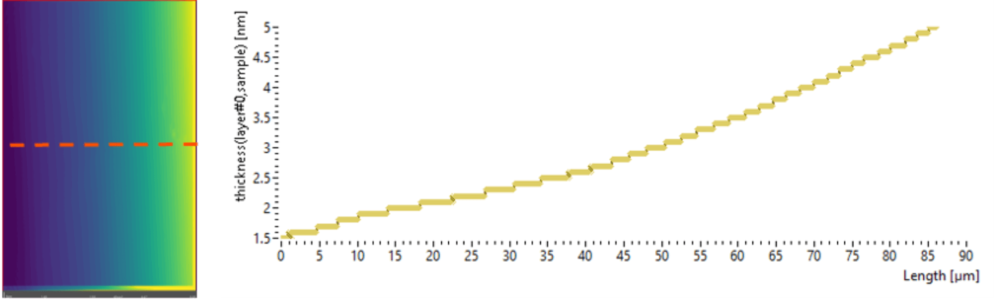
Staircase Structures-Nano steps
- Step Height: 0.3 nm
- Step Width: 3 microns
DALP® technology enables the creation of precise staircase structures with a step height of 0.3 nm and a step width of 3 microns. This precision is essential for applications requiring highly detailed and accurate surface structuration.
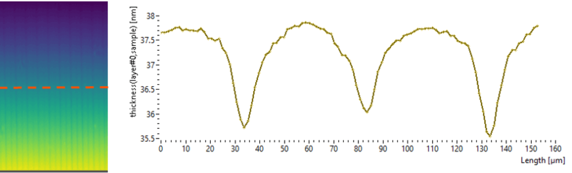
Smooth Valleys
- Height: 1.5 nm
The ability to create smooth valleys with a height of just 1.5 nm, repeated accurately, demonstrates DALP®’s capability in achieving finely tuned surface profiles, which are critical for various advanced applications.
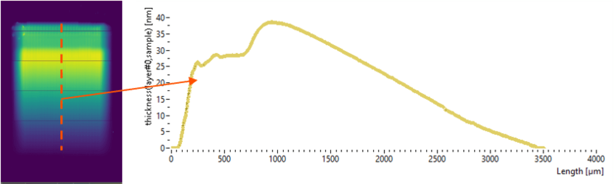
Tapered Shape Structures- Gradients
DALP® also excels in creating tapered shape structures, which are essential for optimizing various micro and nanodevice functionalities. This flexibility in structuring materials at the atomic level opens up new possibilities for innovation in material science.
Efficiency and Innovation
DALP® technology not only simplifies the process of material deposition but also significantly enhances the efficiency of manufacturing workflows. By eliminating the need for vacuum environments, it reduces both the time and costs associated with traditional fabrication methods. This innovation is crucial for advancing research and development in various fields, from microelectronics to photonics and beyond.
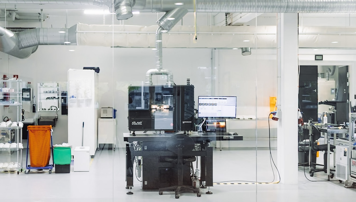
Request a demo of the NANOFABRICATOR™ platform here: https://atlant3d.com/request-a-demo/.
Surface Structuration Information
DATE:
LOCATION: