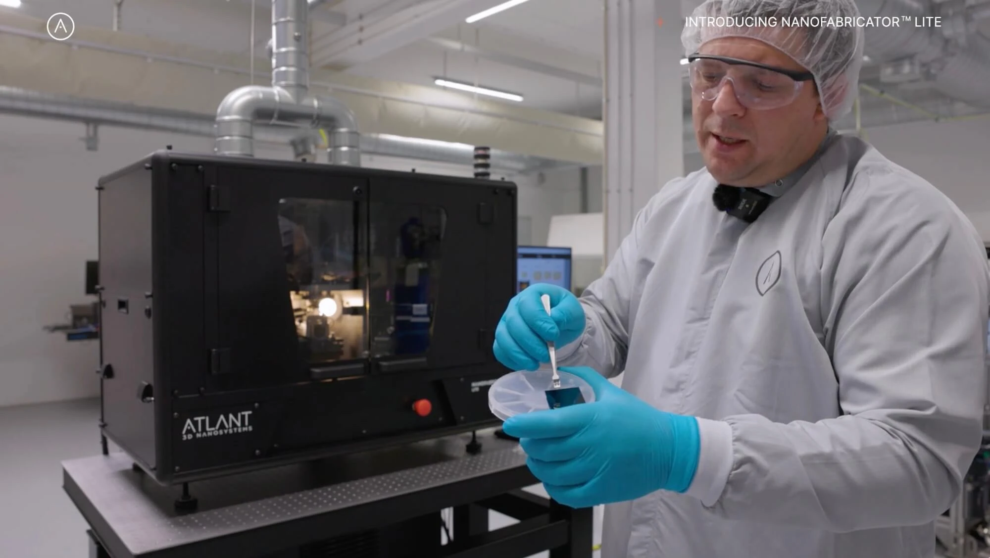
Pioneering new frontiers in space technology Climate change, security and telecoms are among the key themes driving a boom in the space economy. Satellite operators see value across all three orbital altitudes—GEO, MEO and LEO (Geostationary Equatorial Orbit, Medium Earth Orbit and Low Earth Orbit, respectively)—with companies taking different approaches to blending them. GEO still underpins the industry, but telecoms also want to provide differentiated broadband services with integrated, seamless offerings for consumer, business and government customers. Amid LEO constellation programs, the telecom industry continues to debate optimal satellite constellation design and the best end markets. They are also taking different approaches to the various markets, such as aerospace, in-flight connectivity for commercial airlines, maritime communications, navigation and whole new markets such as 5G NTN where roaming between terrestrial and satellite networks are the focus. This “New Space” paradigm demands advanced packaging technologies both adapted to specific requirements and with access from low to medium production scale. At TAS, they defined a packaging roadmap to fit with this new market policy. Our vision is to address in this project a whole new concept applicable to implementing high integration, high thermal and RF performances Front-End Radiating Module. Direct Atomic Layer Processing has been developed by ATLANT 3D Nanosystems [15]. This process is based on selective deposition at the atomic scale of multiple materials like ceramics and metals on many surfaces, from simple to complex shaped ones (Figure 23). This process allows a high conformal deposition and multi-material stacking. This process is well suited to realize multiple functions on MMIC chip surfaces or on electronic packaging internal/external surfaces (example: ceramic housing to encapsulate RF chips) like antenna patterns, EMI shielding, protective coatings, passives elements (example: decoupling capacitors) or thermal interfaces.
![]() Public Funding Project
Public Funding Project Advanced Packaging for RF Modules

![]()
Explore more projects